Method For Releasing a Thin-Film Substrate

Active Publication Date: 2010-11-04
BEAMREACH SOLAR INC
View PDF99 Cites 29 Cited by
  • Summary
  • Abstract
  • Description
  • Claims
  • Application Information

AI Technical Summary

Benefits of technology

[0090]The porous silicon layer may comprise, for example, a first thin porous silicon layer on top and first formed from the bulk silicon of the silicon wafer template. The first thin layer has a low porosity of 15%˜30%. A second thin porous silicon layer is directly grown from the bulk silicon of wafer template and is underneath the first thin layer of porous silicon. The 2nd thin porous silicon layer has a high porosity in the range of 60%˜85%. The top low porosity layer is used as a seed layer for high quality epitaxial silicon growth (for the formation of the epitaxial silicon layer forming the TFSS) and the underneath high porosity silicon layer is used for easier release of the epitaxial silicon layer forming the TFSS. Before the epitaxial silicon growth, the wafer is baked in a high temperature hydrogen environment within the e

Problems solved by technology

However, current limitations stemming from production and manufacturing methods, limited efficiencies, and a lack of infrastructure limit solar cell use.
Counter-intuitively, increases in the efficiencies of solar cell modules often increase the cost of energy ($/Kwh) from those modules.
Increased manufacturing complexity, increased material cost, and yield dominate the cost per module of high efficiency solar cells and limit their cost-effectiveness.
In the past, producing light trapping features employed photolithography and ineffective etching methods, resulting in increased manufacturing cost, complexity, time, and waste.
Additionally

Method used


Image

  • Method For Releasing a Thin-Film Substrate
  • Method For Releasing a Thin-Film Substrate
  • Method For Releasing a Thin-Film Substrate

Examples


Example

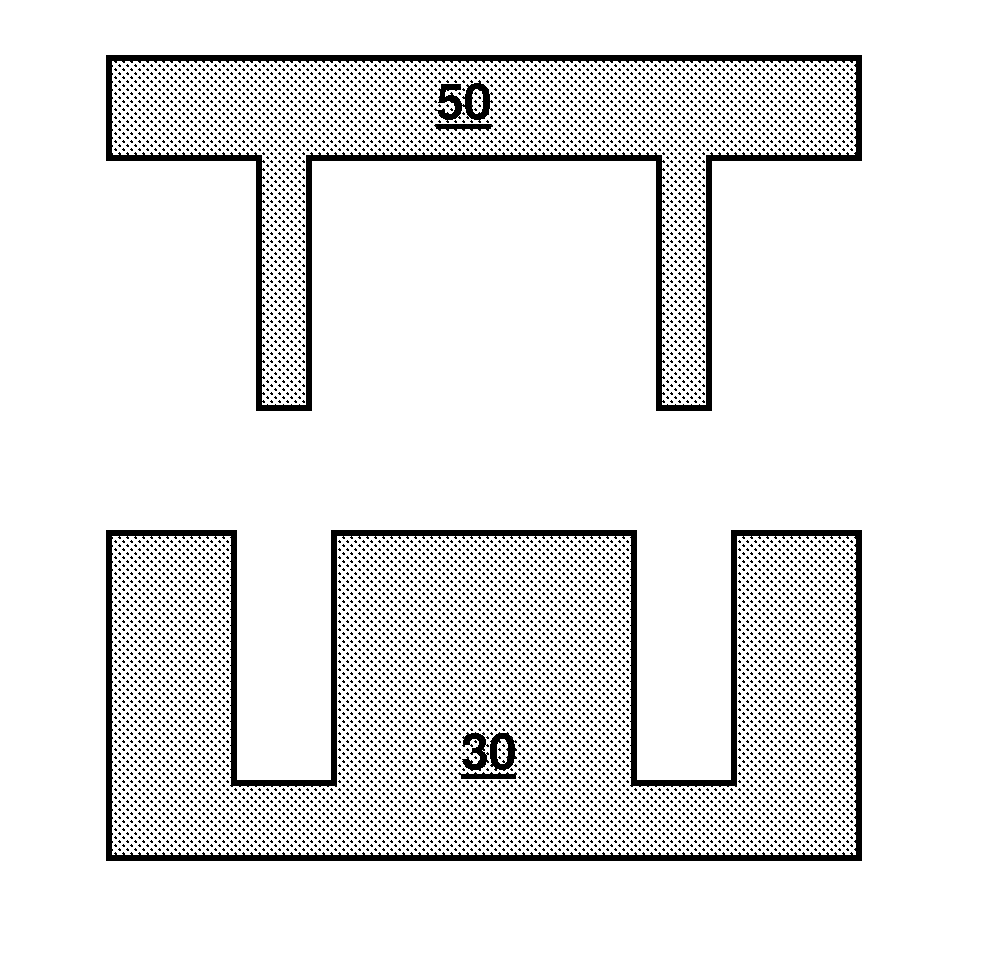
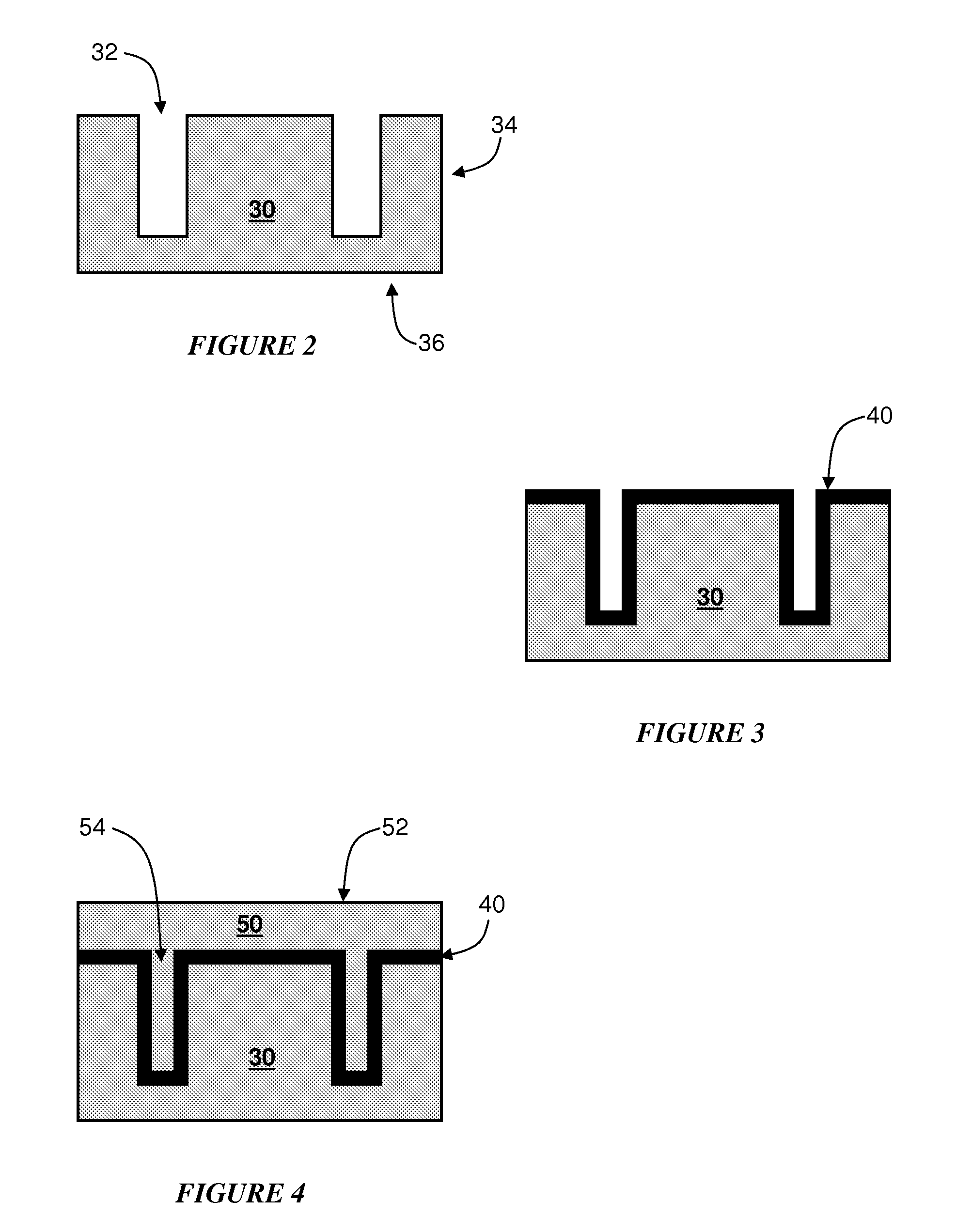
[0035]The following description is not to be taken in a limiting sense, but is made for the purpose of describing the general principles of the present disclosure. The scope of the present disclosure should be determined with reference to the claims. And although described with reference to the manufacture and separation of three-dimensional thin-film semiconductor substrate (TFSS), a person skilled in the art could apply the principles discussed herein to the manufacturing of any multi-dimensional substrate.

[0036]Preferred embodiments of the present disclosure are illustrated in the drawings, like numbers being used to refer to like and corresponding parts of the various drawings. The innovative 3-D TFSS substrate designs and technologies of the current disclosure are based on the use of a three-dimensional, self-supporting, semiconductor thin film, deposited on and released from a reusable crystalline (embodiments include, but are not limited to, monocrystalline or multicrystallin...


PUM


Abstract

The present disclosure relates to methods for selectively etching a porous semiconductor layer to separate a thin-film semiconductor substrate (TFSS) having planar or three-dimensional features from a corresponding semiconductor template. The method involves forming a conformal sacrificial porous semiconductor layer on a template. Next, a conformal thin film silicon substrate is formed on top of the porous silicon layer. The middle porous silicon layer is then selectively etched to separate the TFSS and semiconductor template. The disclosed advanced etching chemistries and etching methods achieve selective etching with minimal damage to the TFSS and template.

Description

CROSS-REFERENCE TO RELATED APPLICATIONS[0001]This application claims priority to and is a continuation in part of pending U.S. patent application Ser. No. 12 / 473,811 “SUBSTRATE RELEASE METHODS AND APPARATUSES” by David Wang and filed on May 28, 2009, which is incorporated herein by reference in its entirety and made part of the present U.S. Utility Patent Application for all purposes.[0002]This application claims priority to and is a continuation in part of pending U.S. patent application Ser. No. 11 / 868,489 “METHODS FOR MANUFACTURING THREE-DIMENSIONAL THIN-FILM SOLAR CELLS”, (U.S. Patent Pub. No. 2008 / 0264477A1) by Mehrdad Moslehi and filed on Oct. 6, 2007, which is incorporated herein by reference in its entirety and made part of the present U.S. Utility Patent Application for all purposes.[0003]This application also claims the benefit of provisional patent application 61 / 158,223 filed on Mar. 6, 2009, which is hereby incorporated by reference in its entirety made part of the pres...

Claims


Application Information

Patent Timeline
IPC IPC(8): H01L21/20
CPCH01L31/18H01L21/30608
Inventor WANG, DAVID XUAN-QIMOSLEHI, MEHRDAD M.RICOLCOL, RAFAELKRAMER, JOE
Owner BEAMREACH SOLAR INC
Why Eureka
Try Eureka