Copper deposition for filling features in manufacture of microelectronic devices

a microelectronic device and copper deposition technology, applied in the direction of liquid/solution decomposition chemical coating, semiconductor devices, coatings, etc., can solve the problems of increasing difficulty in meeting requirements, disturbing electrical characteristics, and severe penalizing the overall performance of the structure, so as to improve the quality of copper deposition and simplify the deposition process

Active Publication Date: 2010-11-11
MACDERMID ENTHONE INC
View PDF11 Cites 37 Cited by
  • Summary
  • Abstract
  • Description
  • Claims
  • Application Information

AI Technical Summary

Benefits of technology

[0016]It is an object of the invention, therefore, to simplify deposition of copper into electrical interconnects, improve the quali

Problems solved by technology

The trend to smaller chip sizes and increased circuit density requires the miniaturization of interconnect features, which severely penalizes the overall performance of the structure because of increasing interconnect resistance and reliability concerns such as electromigration.
First, copper has a tendency to diffuse into the semiconductor's junctions, thereby disturbing their electrical characteristics.
As the architecture of ICs continues to shrink, this requirement proves to be increasingly difficult to satisfy.
The overplating poses challenges for later chemical and mechanical polishing processes that planarize the Cu surface.
In addition to superfilling and overplating issues, micro-defects may form when electrodepositing Cu for filling interconnect features.
One defect that can occur is the formation of internal voids inside the features.
Moreover, smaller size or higher aspect ratio features tend to have thinner seed coverage on the sidewall and bottom of a via/trench where voids can also be produced due to insufficient copper growth in these areas.
An internal void

Method used


Image

  • Copper deposition for filling features in manufacture of microelectronic devices
  • Copper deposition for filling features in manufacture of microelectronic devices
  • Copper deposition for filling features in manufacture of microelectronic devices

Examples


example 1

Copper Metallization of Trenches

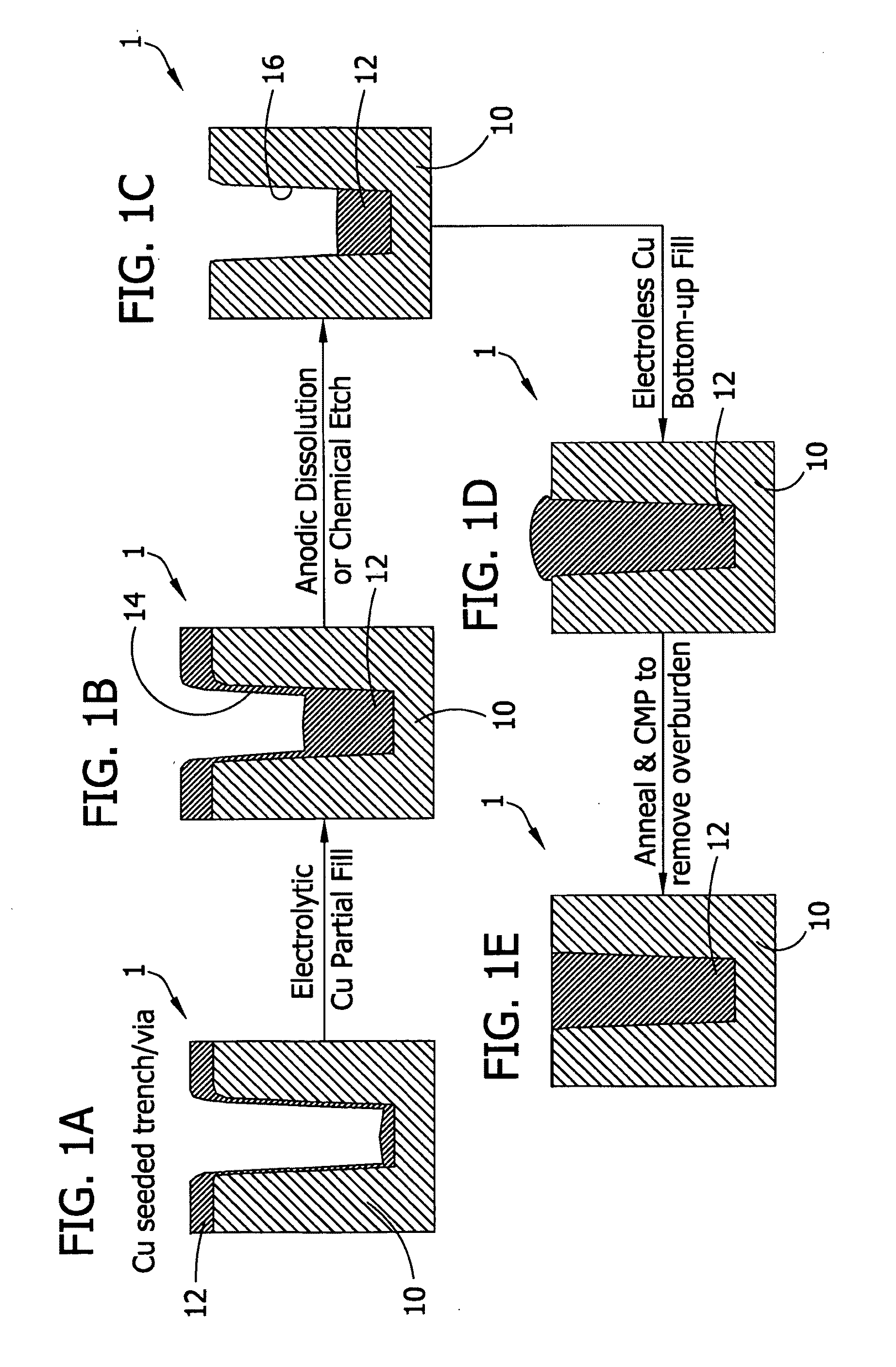
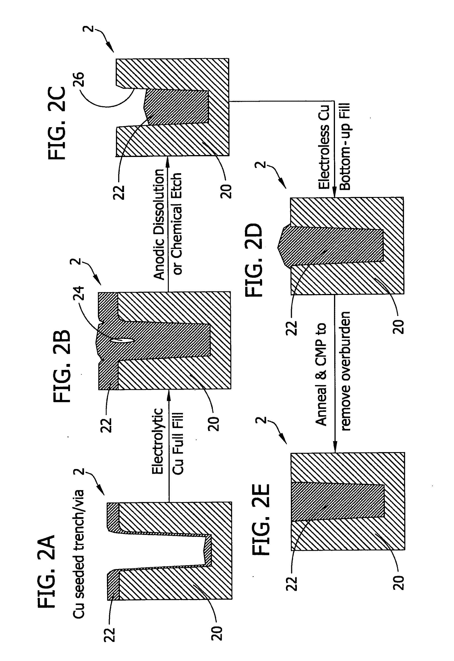
[0064]The process described in connection with FIGS. 1A through 1E was carried out and SEM images were obtained at various points in the process. FIG. 7 is a SEM image taken after electrolytic copper partial fill, and shows the damascene copper deposit is thickest on the bottom with a limited amount of growth on the side walls and top field. This was performed at 10 mA / cm2 current density for 30 seconds with ViaForm® LA Makeup chemistry available from Enthone Inc. of West Haven, Conn. with 6 mL / L ViaForm® Extreme accelerator and 2 mL / L ViaForm® Extreme suppressor. The chemical etching step to achieve the substrate depicted in FIG. 1C was then performed by 20 minutes immersion in saturated (NH4)2CO3 to yield the workpiece shown in the SEM image of FIG. 8. All the copper is removed from the sidewalls and top field, and residual copper is retained on the bottom of the features. FIG. 9 is a SEM image showing the results of electroless Cu bottom-up fill st...


PUM

PropertyMeasurementUnit
Depthaaaaaaaaaa
Depthaaaaaaaaaa
Nanoscale particle sizeaaaaaaaaaa

Abstract

A method for plating copper onto a semiconductor integrated circuit device substrate by forming an initial metal deposit in the feature which has a profile comprising metal on the bottom of the feature and a segment of the sidewalls having essentially no metal thereon, electrolessly depositing copper onto the initial metal deposit to fill the feature with copper. A method for plating copper onto a semiconductor integrated circuit device substrate by forming a deposit comprising a copper wettable metal in the feature, forming a copper-based deposit on the top-field surface, and depositing copper onto the deposit comprising the copper wettable metal to fill the feature with copper.

Description

FIELD OF THE INVENTION[0001]This invention relates to copper deposition for filling of features such as trenches and vias in microelectronic devices.BACKGROUND OF THE INVENTION[0002]An integrated circuit (IC) contains a collection of electrical devices, such as transistors, capacitors, resistors, and diodes, within a dielectric material on a semiconductor substrate. Conductive interconnects connecting discrete devices are referred to as trenches. Additionally, two or more conductive layers, each separated by a dielectric, are typically employed within a given IC to increase its overall performance.[0003]Conductive interconnects known as vias are used to connect these distinct conductive layers together. Currently, ICs typically have silicon oxide as the dielectric material and copper as the conductive material.[0004]The demand for manufacturing semiconductor IC devices such as computer chips with high circuit speed, high packing density and low power dissipation requires the downwar...

Claims


Application Information

Patent Timeline
IPC IPC(8): H01L21/768
CPCC25D5/02C25D7/123C25D5/54H01L21/288H01L21/2885H01L21/76843H01L21/76865H01L21/76873H01L21/76874H01L21/76877H01L21/76879C23C18/1879C23C18/1896C23C18/1608C23C18/1653C23C18/40C23C18/405C25D5/48
Inventor LIN, XUANHURTUBISE, RICHARDPANECCASIO, JR., VINCENTCHEN, QINGYUN
Owner MACDERMID ENTHONE INC
Why Eureka
Try Eureka