Buffer circuit, image sensor chip comprising the same, and image pickup device
- Summary
- Abstract
- Description
- Claims
- Application Information
AI Technical Summary
Benefits of technology
Problems solved by technology
Method used
Image

Examples
first embodiment
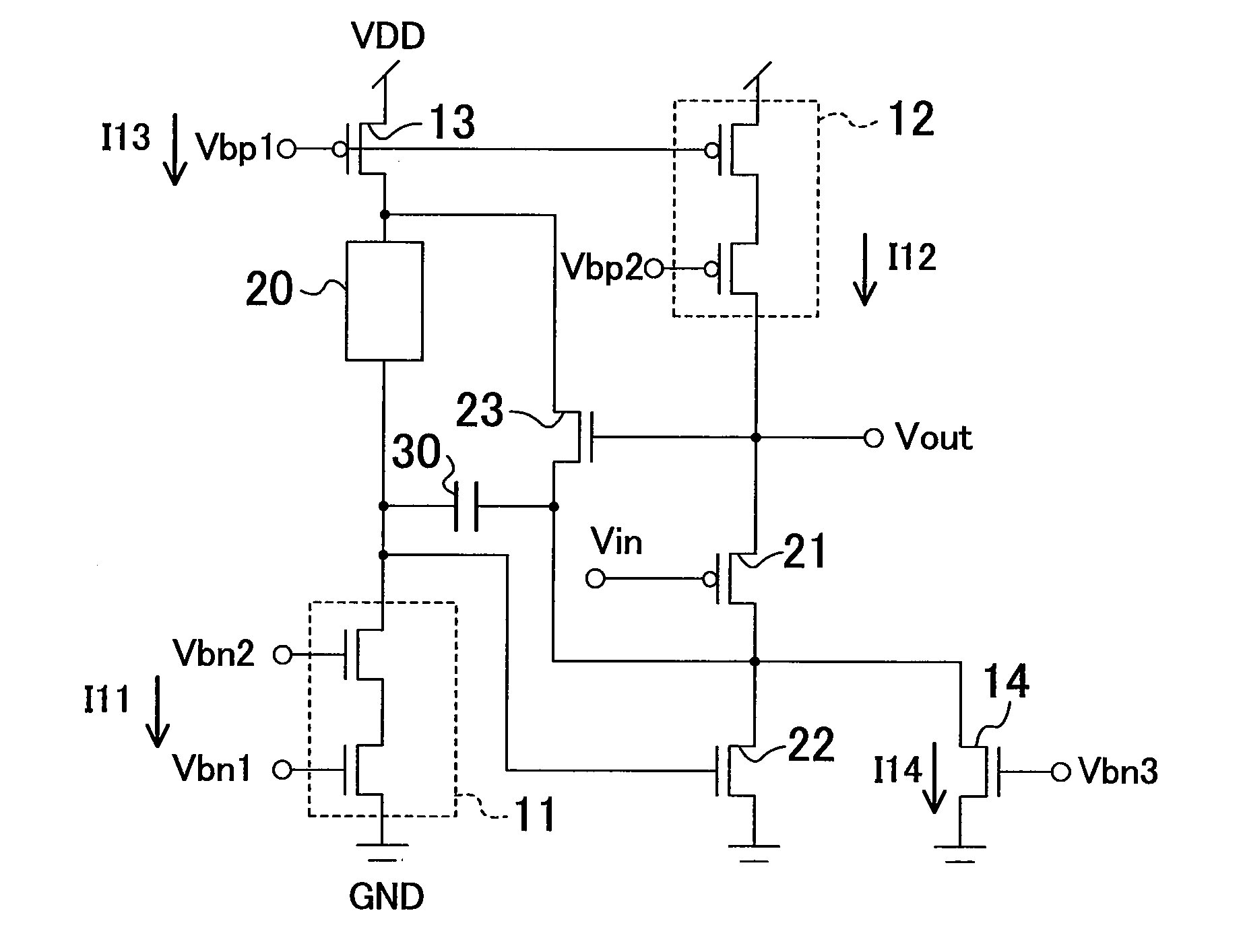
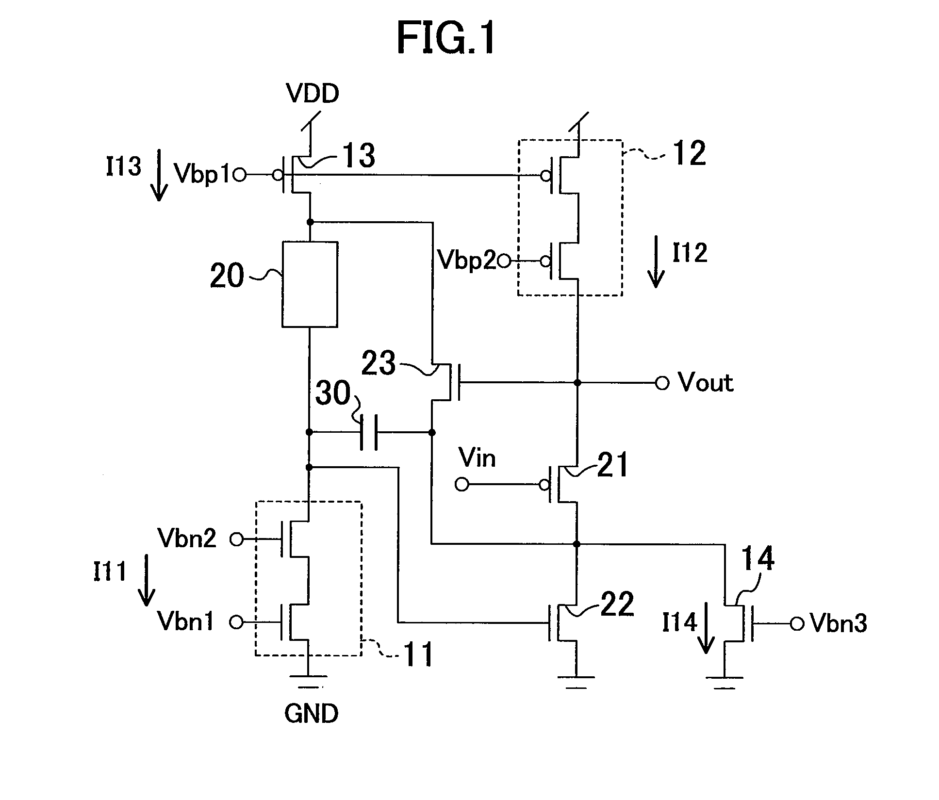
[0044]FIG. 1 illustrates a configuration of a buffer circuit according to a first embodiment. The buffer circuit can be fabricated in a CMOS process. A cascode constant current source 11 includes two cascode-connected NMOS transistors, where bias voltages Vbn1 and Vbn2 are applied to respective gates of the NMOS transistors. The cascode constant current source 11 supplies a constant current Ill. A cascode constant current source 12 includes two cascode-connected PMOS transistors, where bias voltages Vbp1 and Vbp2 are applied to respective gates of the PMOS transistors. The cascode constant current source 12 supplies a constant current I12. A constant current source 13 includes a PMOS transistor, where the bias voltage Vbp1 is applied to the gate of the PMOS transistor. The constant current source 13 supplies a constant current I13.
[0045]One end of a resistive load 20 is connected to an output of the cascode constant current source 11, and the other end of the resistive load 20 is co...
second embodiment
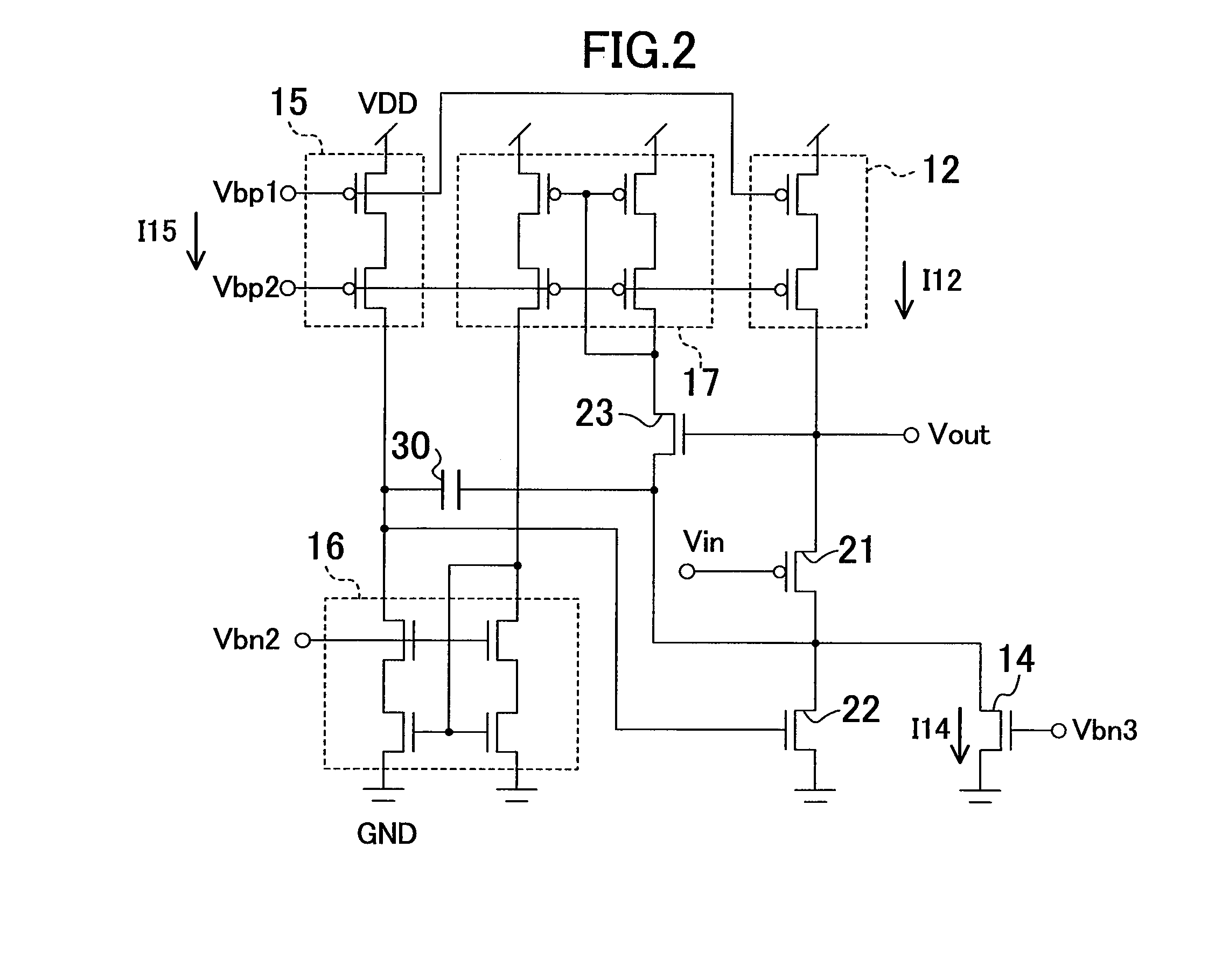
[0051]FIG. 2 illustrates a configuration of a buffer circuit according to a second embodiment. The buffer circuit can also be fabricated in a CMOS process. Cascode constant current sources 12 and 15 each include two cascode-connected PMOS transistors, where bias voltages Vbp1 and Vbp2 are applied to respective gates of the PMOS transistors. The cascode constant current source 12 supplies a constant current I12. The cascode constant current source 15 supplies a constant current I15.
[0052]A cascode current mirror circuit 16 includes two cascode-connected NMOS transistors on each of its input side and output side, where a bias voltage Vbn2 is applied to the gate of the NMOS transistor of a cascode stage on the input side and to the gate of the NMOS transistor of a cascode stage on the output side. A cascode current mirror circuit 17 includes two cascode-connected PMOS transistors on each of its input side and output side, where the bias voltage Vbp2 is applied to the gate of the PMOS t...
third embodiment
[0060]FIG. 3 illustrates a configuration of a buffer circuit according to a third embodiment. The buffer circuit can also be fabricated in a CMOS process. Cascode constant current sources 12 and 15 each include two cascode-connected PMOS transistors, where bias voltages Vbp1 and Vbp2 are applied to respective gates of the PMOS transistors. The cascode constant current source 12 supplies a constant current I12. The cascode constant current source 15 supplies a constant current I15.
[0061]The source of a PMOS transistor 21 is connected to an output of the cascode constant current source 12. The input signal Vin of the buffer circuit is applied to the gate of the PMOS transistor 21, and the output signal Vout of the buffer circuit is output from the source of the PMOS transistor 21. That is, the PMOS transistor 21 operates as a source follower biased with the constant current I12.
[0062]The drain of an NMOS transistor 22 is connected to the drain of the PMOS transistor 21. The source of ...
PUM
 Abstract
Description
Claims
Application Information
 - R&D
- Intellectual Property
- Life Sciences
- Materials
- Tech Scout
- Unparalleled Data Quality
- Higher Quality Content
- 60% Fewer Hallucinations
Browse by: Latest US Patents, China's latest patents, Technical Efficacy Thesaurus, Application Domain, Technology Topic, Popular Technical Reports.
© 2025 PatSnap. All rights reserved.Legal|Privacy policy|Modern Slavery Act Transparency Statement|Sitemap|About US| Contact US: help@patsnap.com