Organic electroluminescence device

a technology of electroluminescence device and organic material, which is applied in the direction of electroluminescent light source, chemistry apparatus and process, and composition of light source, can solve the problems of limited examples that achieved a practical life and efficiency, material unadjustable deformation, and decreased luminance, and achieve excellent color stability

Inactive Publication Date: 2010-11-25
IDEMITSU KOSAN CO LTD
View PDF13 Cites 39 Cited by
  • Summary
  • Abstract
  • Description
  • Claims
  • Application Information

AI Technical Summary

Benefits of technology

[0017]An object of the invention is to provide an organic EL device excellent in color stability at the time of changes in current density and also at the time of continuous driving.
[0025]According to the aspect of the invention, the fused polycyclic aromatic derivatives contained in the first emitting layer and the second emitting layer have high resistance against carriers from the anode or the cathode. Thus, the third emitting layer interposed therebetween is not degraded by carriers.
[0026]Accordingly, the degradation of the compound(s) contained in the third emitting layer can be suppressed, and such a level of Eg(T) as required for higher-efficiency phosphorescent emission can be stably obtained. Thus, not only at the time when current density is changed but also at the time when the device is continuously driven, the organic electroluminescence device can exhibit excellent color stability and high luminous efficiency.
[0028]The aspect of the invention is capable of providing an organic EL device excellent in color stability at the time of changes in current density and also at the time of continuous driving.

Problems solved by technology

However, a variety of challenges have been noted in practical realization, among which, for instance, organic EL devices are indispensably required to reduce its power consumption when used as illuminators.
However, there have been few examples that achieved a practical lifetime and efficiency.
As a reason for the above, as degradation of materials is progressed in accordance with driving of the device, luminance is decreased and the materials become unequally degraded, whereby color shift and the like come to a big issue.
Further, when organic EL devices are applied to illuminators or displays, white-emitting devices are required.
However, Document 1 or 2 has no disclosure on color shift resultant from continuous driving, which is another big issue in white-emitting devices in practice.
However, although having high Eg(T), such heterocycle-containing skeletons are less stable against oxidation and reduction and vulnerable to degradation due to accumulated carrier.
In other words, when degradation of materials due to accumulated carrier occurs at an interface between the emitting layer and peripheral materials of layers adjoining to the emitting layer, carrier balance may be changed due to driving and balance of emitting colors may be deteriorated, which may lead to color shift.

Method used


Image

  • Organic electroluminescence device
  • Organic electroluminescence device
  • Organic electroluminescence device

Examples


example 1

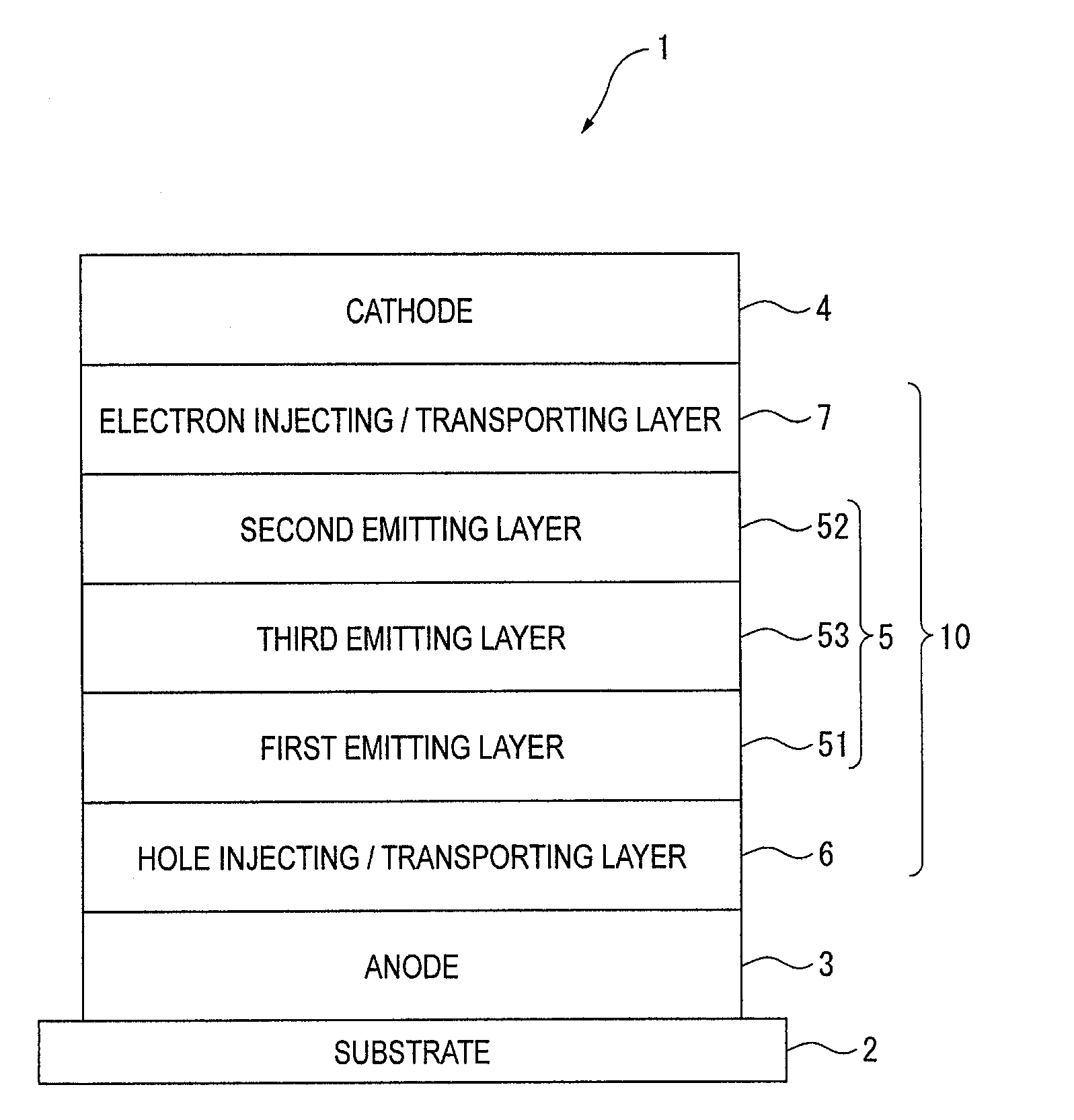
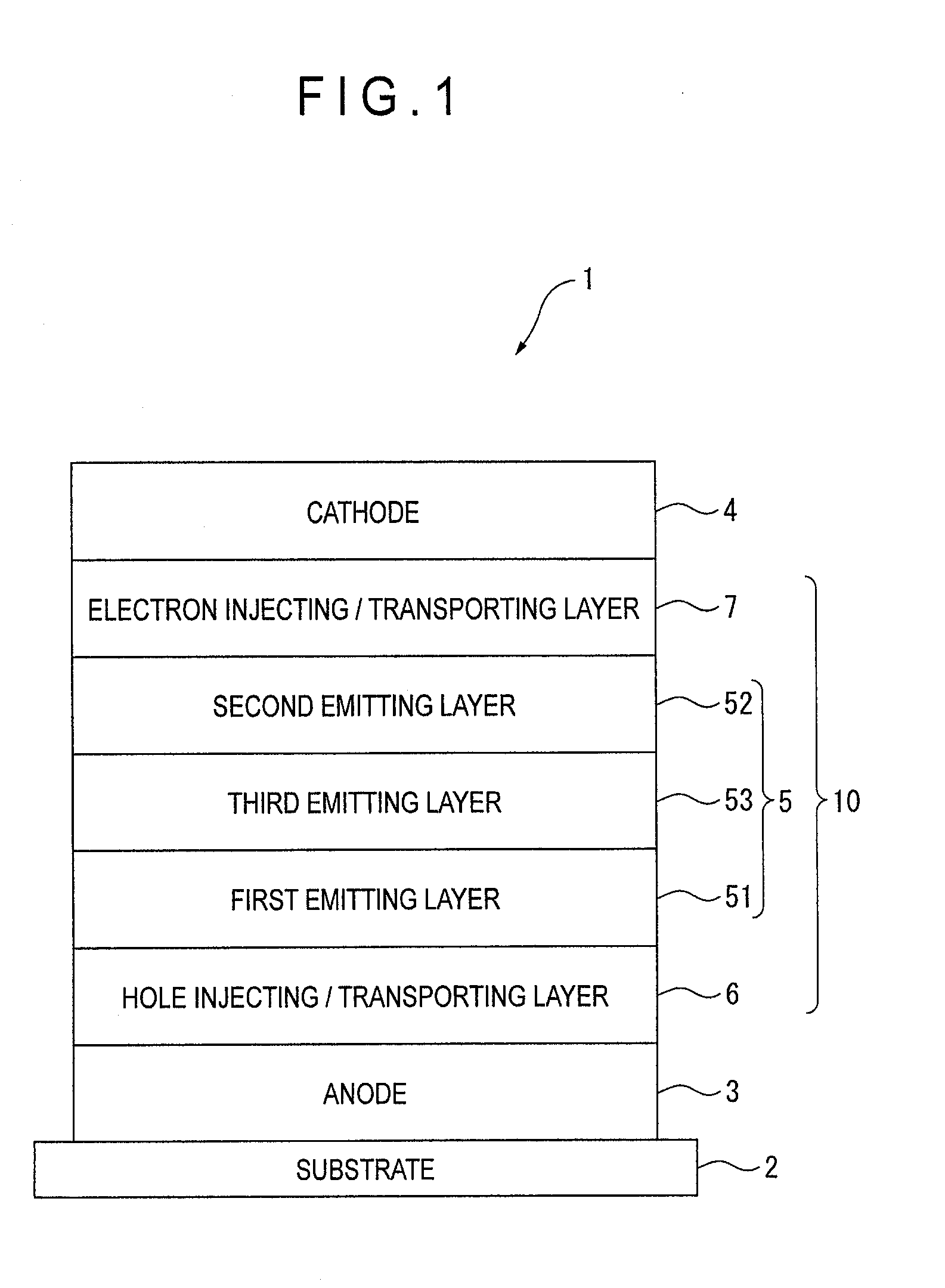
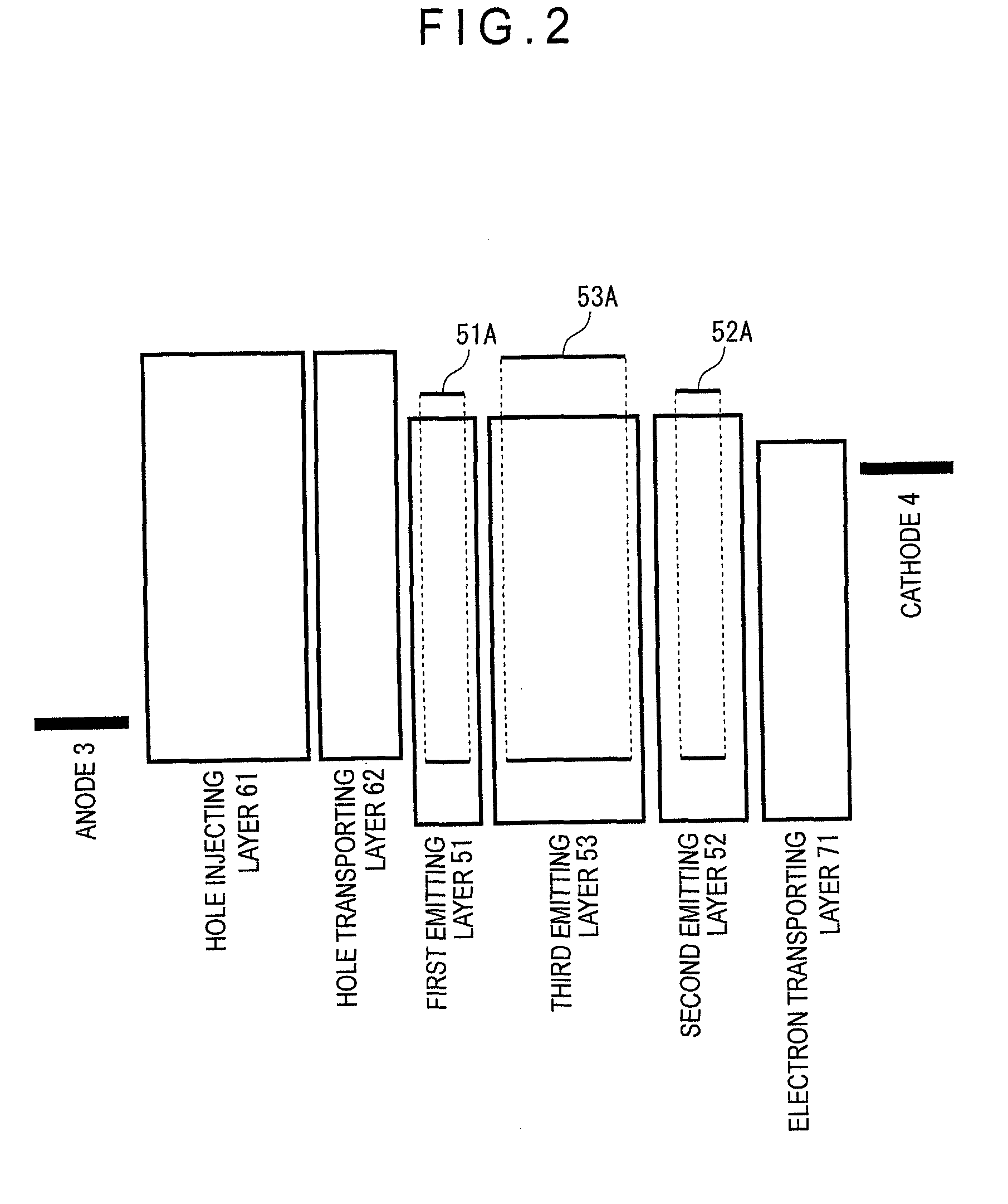
[0303]A glass substrate (size: 25 mm×75 mm×1.1 mm thick, manufactured by Geomatec Co., Ltd.) having an ITO transparent electrode (anode) was ultrasonic-cleaned in isopropyl alcohol for five minutes, and then UV / ozone-cleaned for 30 minutes. After the glass substrate having the transparent electrode line was cleaned, the glass substrate was mounted on a substrate holder of a vacuum deposition apparatus, so that a 10-nm thick film of a compound HT1 was initially formed at 1 Å / s as a hole injecting layer on a surface of the glass substrate where the transparent electrode line was provided so as to cover the transparent electrode.

[0304]On this film, a 10-nm thick film of a compound HT2 was formed at 1 Å / s as a hole transporting layer.

[0305]Further on this film of the compound HT2, a 3-nm thick film of a compound L1 and compound D1 was formed as a first emitting layer with a thickness ratio of the compound L1 to D1 being 2.85:0.15. Film-forming rates were respectively 1 Å / s and 0.052 Å / s...

example 2

[0311]Except that the compound L3 was used as the second emitting layer in place of the compound L1, the organic EL device according to Example 2 was manufactured in the same manner as Example 1.

example 3

[0312]A glass substrate (size: 25 mm×75 mm×1.1 mm thick, manufactured by Geomatec Co., Ltd.) having an ITO transparent electrode (anode) was ultrasonic-cleaned in isopropyl alcohol for five minutes, and then UV / ozone-cleaned for 30 minutes. After the glass substrate having the transparent electrode line was cleaned, the glass substrate was mounted on a substrate holder of a vacuum deposition apparatus, so that 10-nm thick film of the compound HT1 was initially formed at 1 Å / s as a hole injecting layer on a surface of the glass substrate where the transparent electrode line was provided so as to cover the transparent electrode.

[0313]On this film, a 10-nm thick film of the compound HT2 was formed at 1 Å / s as a hole transporting layer.

[0314]Further on this film of the compound HT2, a 3-nm thick film of the compound L1 and compound D1 was formed as a first emitting layer with a thickness ratio of the compound L1 to D1 being 2.85:0.15. Film-forming rates were respectively 1 Å / s and 0.052...


PUM

PropertyMeasurementUnit
triplet energyaaaaaaaaaa
work functionaaaaaaaaaa
thicknessaaaaaaaaaa

Abstract

An organic electroluminescence device includes: an anode; a cathode; and an organic thin-film layer provided between the anode and the cathode and including at least three emitting layers. The organic thin-film layer includes: a first emitting layer adjacent to the anode; a second emitting layer adjacent to the cathode; and a third emitting layer interposed between the first emitting layer and the second emitting layer. The first emitting layer, the second emitting layer and the third emitting layer contain phosphorescent dopants. The first emitting layer and the second emitting layer use fused polycyclic aromatic derivatives as host materials.

Description

BACKGROUND OF THE INVENTION[0001]1. Field of the Invention[0002]The present invention relates to an organic electroluminescence device.[0003]2. Description of Related Art[0004]Organic electroluminescence devices (hereinafter abbreviated as “organic EL device”), which include organic thin-film layers (in which emitting layers are included) between anodes and cathodes, have been known to emit light using exciton energy generated by recombination a of holes and electrons that have been injected into the emitting layers.[0005]Such an organic EL device, which has the advantages as a self-emitting device, is expected to serve as an emitting device excellent in luminous efficiency, image quality, power consumption and thin design.[0006]However, a variety of challenges have been noted in practical realization, among which, for instance, organic EL devices are indispensably required to reduce its power consumption when used as illuminators.[0007]One method of reducing the power consumption i...

Claims


Application Information

Patent Timeline
Patent Type & Authority Applications(United States)
IPC IPC(8): H01L51/10
CPCC09K11/06C09K2211/1011H05B33/14H10K85/636H10K85/6574H10K85/342H10K85/6572H10K50/125H10K50/11H10K2101/10
Inventor KAWAMURA, YUICHIRONISHIMURA, KAZUKIJINDE, YUKITOSHIKUMA, HITOSHIOGIWARA, TOSHINARI
Owner IDEMITSU KOSAN CO LTD
Why Eureka
Try Eureka