

Optical structure to reduce internal reflections
- Summary
- Abstract
- Description
- Claims
- Application Information
AI Technical Summary
Benefits of technology
Problems solved by technology
Method used
Image

Examples
embodiment one
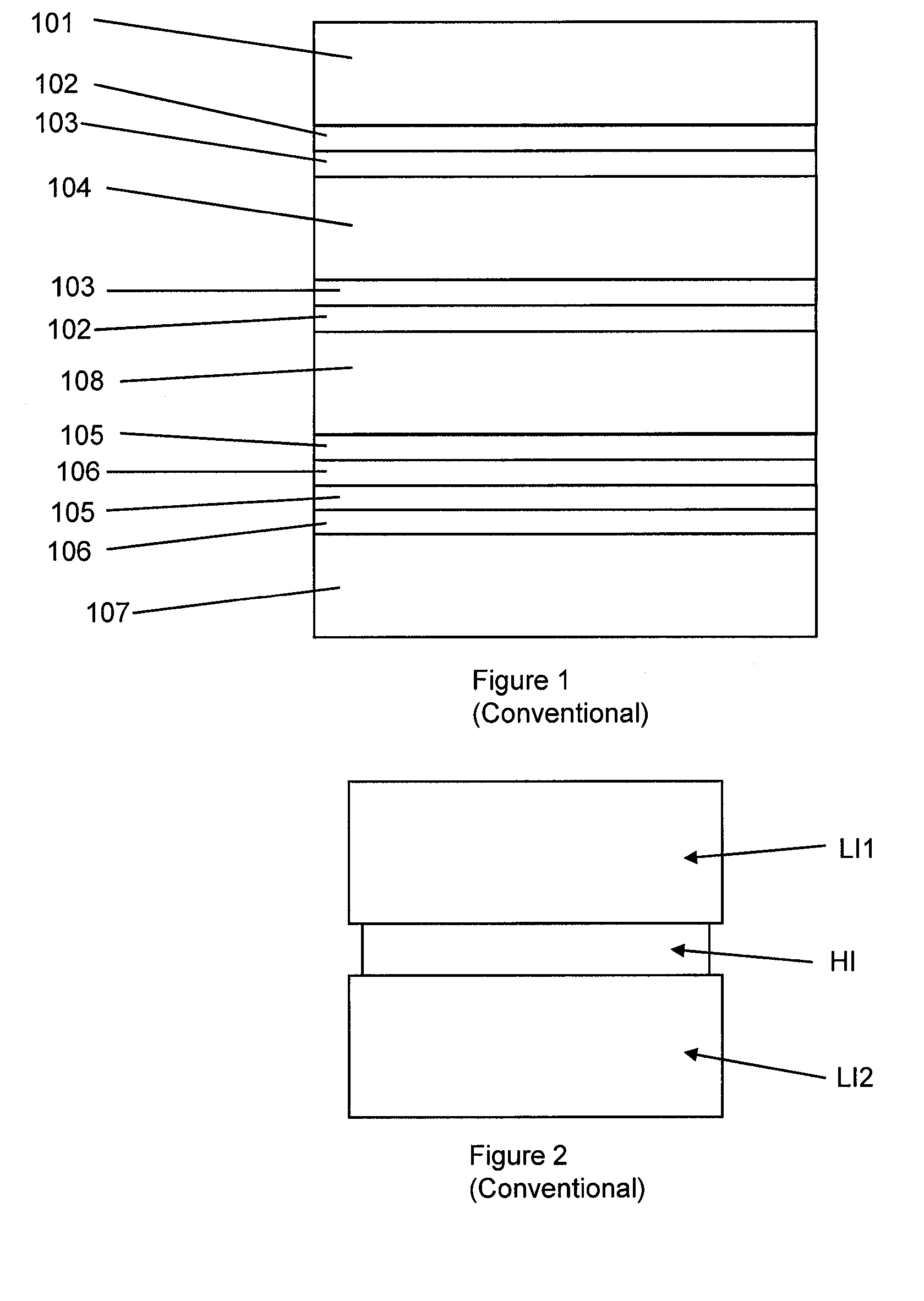
[0054]Referring to FIG. 1, there is shown an example of an optical structure embodied as a liquid crystal display (LCD), where one ITO electrode, 102, with n≈1.95, lies between layers of liquid crystal (LC), 104, with n≈1.53, and glass or color filter (CF), 101, with n≈1.53, and the other lies between LC, 104 and a planarizing resin, 108, with n≈1.59. There is also a thin layer of polyimide (PI), 103, with n≈1.70, between the LC and each ITO electrode. There are also layers of silicon nitride, 105, with n≈2.04, between layers of silica, 106, with n≈1.55 and / or the planarizing resin. The silica and silicon nitride layers are used as dielectric and for passivation in and around the TFT system. Glass, 107, supports the structure. This is one typical structure in use in the industry, and is also described in Table 1, with thickness also given for each layer.
TABLE 1Label inRefractive indexMaterialFIG. 1(approximate)ThicknessColor filter (CF)1011.50>10 μmITO1021.95138 nmPolyimide (PI)1031...
embodiment 2
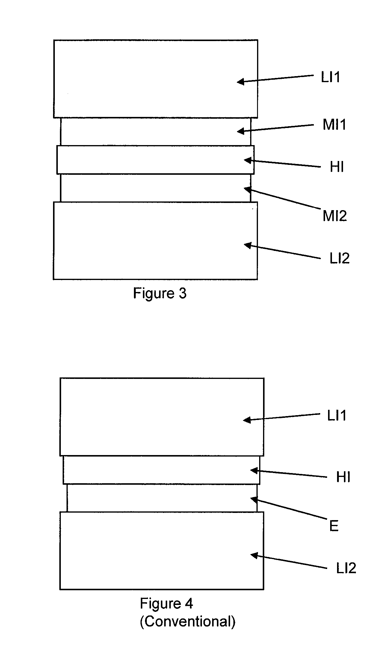
[0060]It is also possible to remove the silica and / or silicon nitride from the areas through which light is transmitted in an LCD. This is because they are only required around the TFT and circuitry in the device. Light is not transmitted through these regions (it is either reflected by metal or absorbed in the commonly used black mask), and so they can be considered irrelevant for purposes of reducing internal reflections. The silica and silicon nitride can in principle be patterned so that they are only found in these opaque regions, not in the transparent part of the pixel. In this case, the structure is as given in Table 4 and FIG. 7.
[0061]The structure described in Table 3 has the thicknesses of PI and ITO optimized to minimize total reflectivity by destructive interference. The total reflectivity of this structure is 0.015; 1.5% of incident light is reflected by this internal structure.
TABLE 4Label inRefractive indexMaterialFIG. 7(approximate)ThicknessColor filter (CF)1011.50>...
PUM
 Abstract
Description
Claims
Application Information