Method for fabrication of thin film phosphor, thin film phosphor, and phosphor prouct using the same

a technology of phosphor and phosphor, which is applied in the field can solve the problems of small reduction in light emission efficiency, light loss, and lowering the effect of thin film phosphor, and achieve excellent transmission rate, light emission properties, and reduced manufacturing costs.

Inactive Publication Date: 2010-11-11
LUCIMEA
View PDF4 Cites 4 Cited by
  • Summary
  • Abstract
  • Description
  • Claims
  • Application Information

AI Technical Summary

Benefits of technology

[0027]According to the present invention, some of constitutional elements for a phosphor are used for a substrate while all or other constitutional elements except for those used for the substrate are used as a raw material, thereby enabling formation substantially all types of thin film phosphors. Consequently, such fabricated thin film phosphors may be employed in a wide range of applications without limitation to display products. Also, the thin film phosphor has light emission properties equal to those of a powder phosphor and excellent transmission rate, thus being effectively applied to a fluorescent sheet for OLED color conversion, a fluorescent plate for X-Ray device or electron microscope, etc., in addition to light emitting FPDs described above.
[0028]Moreover, the method for fabrication of a thin film phosphor according to the present invention may be used for a large-scale substrate and may considerably reduce manufacturing costs thereof.

Problems solved by technology

A principal cause of lowering effects of the thin film phosphor is light loss due to total internal reflection of 80 to 90% light.
For a powder phosphor, since light is emitted outside after internal reflection several times, the total internal reflection causes only a small reduction in light emission efficiency.
Although the powder phosphor has excellent light emission efficiency, a display resolution is restricted due to a size of particle, poor reliability and processing difficulties are entailed in patterning, etc.
However, as disclosed above, such a thin film phosphor fabricated by the foregoing methods entails problems of considerably decreased such as light emission efficiency, compared to a powder phosphor.
However, since a FPD uses a glass substrate which cannot be heated at a temperature of more than 600 to 700° C., the thin film phosphor encounters a problem of not being applied to a practical process for manufacturing of FPDs.
Conventional methods for formation of thin film phosphors do not meet a recent tendency to increase in scale of a substrate, a thin film phosphor fabricated by the conventional method has poor luminance, and transparency of the phosphor is not suitably obtained due to interference patterns at a boundary between the phosphor and a substrate and / or light reflection.

Method used


Image

  • Method for fabrication of thin film phosphor, thin film phosphor, and phosphor prouct using the same
  • Method for fabrication of thin film phosphor, thin film phosphor, and phosphor prouct using the same
  • Method for fabrication of thin film phosphor, thin film phosphor, and phosphor prouct using the same

Examples


example 1

Zn2SiO4:Mn2+ Thin Film Phosphor

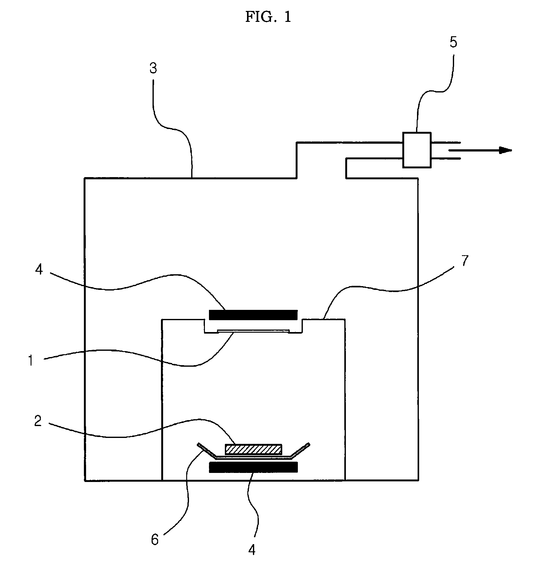
[0071]ZnO and MnO as a raw material and an amorphous quartz substrate are placed in a chamber of an electric furnace. After exhausting the chamber, a ZnO and MnO power mixture is subjected to gas diffusion and reacts with the amorphous quartz substrate while heating the chamber. The treated material as a sample is naturally cooled and completed into a final Zn2SiO4:Mn2+ thin film phosphor.

[0072]In this case, an initial combination pressure inside the chamber ranges from 10−2 to 10−4 Torr and a temperature thereof ranges from 1,000 to 1,200° C. Also, the combination time ranges from 6 to 24 hours. While altering such combination conditions, the thickness of the thin film phosphor (a thickness of the phosphor from an original surface of the substrate before combination) was tested. Tested results are shown in the following Table 4.

TABLE 4Thickness of phosphor layer from original surface ofsubstrate based on different combination conditionsCombination tem...

example 2

BaSi2O5:Eu2+ Thin Film Phosphor

[0086]BaO and Eu2O3 as a raw material and a quartz substrate are prepared and a green emitting BaSi2O5:Eu2+ thin film phosphor is fabricated according to the same procedures in Example 1.

[0087]In this case, after exhausting the chamber under a pressure of 10−4 Torr, the raw material is diffused in a gas state into at 1,200° C., followed by conducting reaction of the raw material with the substrate for 6 hours. Then, the treated material is naturally cooled and completed into a final thin film phosphor.

[0088]The obtained thin film phosphor has a thickness of 3 μm and a relative luminance of 86% in comparison to a powder phosphor.

example 3

ZnAl2O4:Mn2+ Thin Film Phosphor

[0089]ZnO and MnO as a raw material and a sapphire (Al2O3) substrate are prepared and a green emitting ZnAl2O4:Mn2+ thin film phosphor is fabricated according to the same procedures in Example 1.

[0090]In this case, after exhausting the chamber to a pressure of 10−2 Torr, the raw material is diffused in a gas state into at 1,000° C., followed by conducting reaction of the raw material with the substrate for 6 hours. Then, the treated material is naturally cooled and completed into a final thin film phosphor.

[0091]The obtained thin film phosphor has a thickness of 2 μm and a relative luminance of 80% in comparison to a powder phosphor.

[0092]2) Second Combination Process

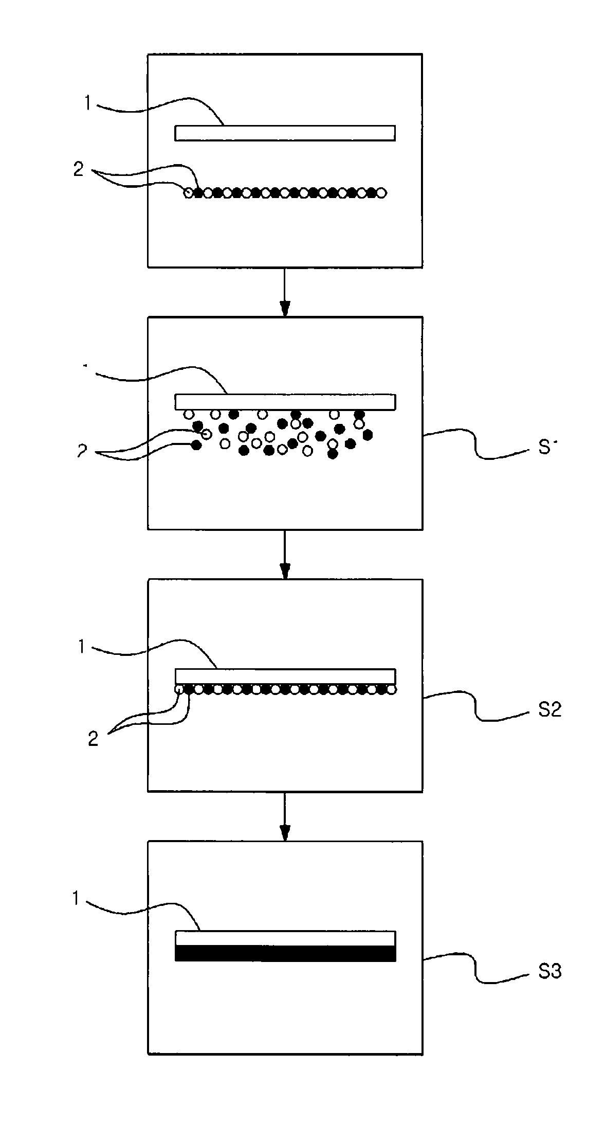
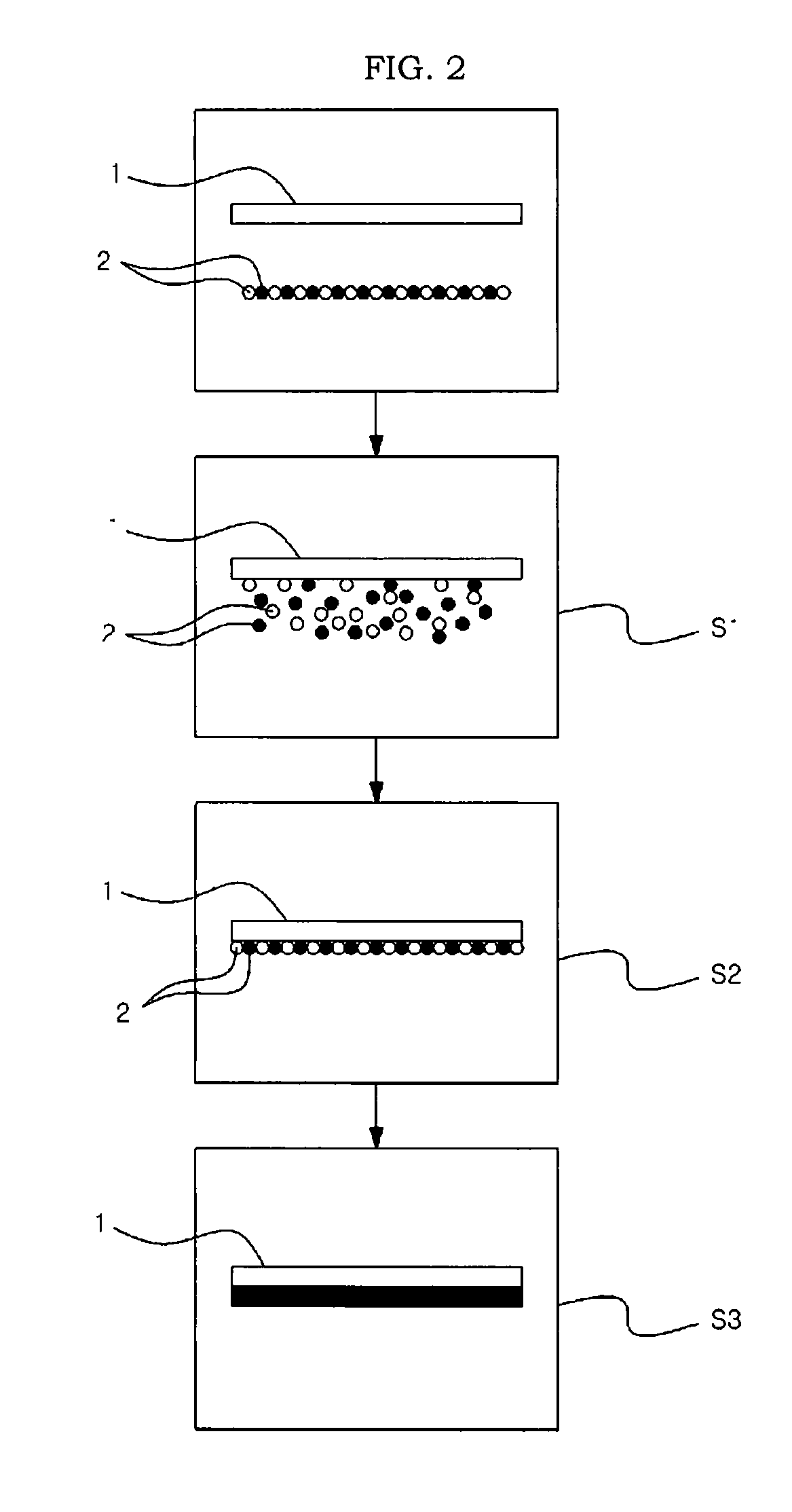
[0093]In contrast to the foregoing first combination process, a second combination process of forming a raw material on a substrate according to the present invention includes depositing the raw material on a surface of the substrate then heating the substrate having the raw material depos...


PUM

PropertyMeasurementUnit
diameteraaaaaaaaaa
temperatureaaaaaaaaaa

Abstract

Disclosed are a method for fabrication of a thin film phosphor, a thin film phosphor and a product using the same. The thin film phosphor is fabricated by adsorbing a raw material to a surface of a substrate simultaneously with diffusing the same or, otherwise, depositing the raw material on the substrate and heating the same, so as to diffuse the raw material from the surface of the substrate into the substrate wherein the substrate contains at least one selected from constitutional elements of the phosphor. The fabricated thin film phosphor has a constitutional composition continuously varied to gradually come close to a constitutional composition of the substrate when the constitutional elements of the phosphor are diffused from a surface to an inner side of the substrate. In particular, if the substrate material, the raw material and the phosphor layer material have the same or similar structure, and when the phosphor layer material has an anisotropic texture structure, light luminance is maximized while a decay time is minimized. According to this disclosure, different thin film phosphors with improved luminance comparable to that of a powder phosphor may be fabricated. Compared to such powder phosphor, the thin film phosphor fabricated as described above is thermally and chemically stable and does not exhibit an interference pattern or light reflection between the thin film phosphor and the substrate so as to have excellent light transmission, thereby being applicable to large-scale display devices.

Description

BACKGROUND OF THE INVENTION[0001]1. Field of the Invention[0002]The present invention relates to a thin film phosphor and, more particularly, a thin film phosphor fabricated by forming a raw material of the phosphor on a surface of a workpiece material such as a substrate, a phosphor product manufactured using the same, and a method for fabrication thereof.[0003]2. Description of the Related Art[0004]Flat panel displays (FPDs) currently developed as an information transmission device are generally classified into light receiving types such as liquid crystal display (LCD) and light emitting types such as plasma display panel (PDP), field emission display (FED), electroluminescence display (ELD), vacuum fluorescent display (VFD), etc. Although the light emitting type FPD is distinguishable into different type devices in terms of structure and light emission source, all of these devices commonly make use of a phosphor. Such phosphor may be divided into a powder phosphor and a thin film...

Claims


Application Information

Patent Timeline
Patent Type & Authority Applications(United States)
IPC IPC(8): F21V9/16B05D3/06B05D5/06B05D3/10
CPCC09K11/595C09K11/642Y10T428/24355H05B33/10C09K11/7734C09K11/77342C09K11/08C09K11/77
Inventor LEE, EUN-WOOKKIM, JONG-SOOPARK, JE-HONG
Owner LUCIMEA
Why Eureka
Try Eureka