Nanowire mesh device and method of fabricating same

a technology of nanowires and meshes, applied in the field of nanowire mesh devices, can solve the problems of difficult contact with nanowires, difficult scaling of gate pitch, and difficult fabrication of nanowires at very tight gate pitch and high density of current-carrying surfaces, etc., to improve the contact scheme and scalability, improve the effect of current-carrying density and improved vertical uniformity in junction profiles

Inactive Publication Date: 2010-11-25
GLOBALFOUNDRIES U S INC
View PDF7 Cites 94 Cited by
  • Summary
  • Abstract
  • Description
  • Claims
  • Application Information

AI Technical Summary

Benefits of technology

[0010]The present invention provides a semiconductor structure, e.g., a nanowire FET structure, which has an improved contact scheme and scalability. Moreover, and in conjunction with these improvements, the present invention provides a semiconductor structure in which the current carrying density is increased. Also, the inventive structure has improved vertical uniformity in junction profiles. As such, the height of the inventive structure (i.e., the number of stacked semiconductor nanowires) is not limited by the ability to define source and drain junctions from a top-down implant. It is yet further observed that the inventive structure has reduced gate-to-source / drain capacitance as compared to prior art FinFET structures since during the inventive process a thin, self-limiting interfacial oxide is typically formed on undoped semiconductor nanowires.

Problems solved by technology

The architecture of a nanowire FET, however, presents notable fabrication challenges.
However, even with deterministic placement, fabrication of nanowires at very tight gate pitch and a high density of a current-carrying surface are challenging.
Scaled gate pitch makes contacting nanowires difficult.
Properly and consistently aligning the landing pads with the gate is nearly impossible at required gate pitches unless a self-aligned scheme is utilized.
Because nanowires are expected to be at a smaller pitch than contact vias for a high layout density technology, nanowire source / drain regions need to be contacted by contact bars; contact bars introduce greater complexity in patterning and typically require the insertion of an extra mask layer between the contact bars and the first metal layer.
Epitaxial processes, however, have drawbacks due to their extreme sensitivity to surface chemistry, crystal orientation and growth conditions.
Achieving a high density of a current carrying surface is the other challenge of making high layout density nanowire FETs.

Method used


Image

  • Nanowire mesh device and method of fabricating same
  • Nanowire mesh device and method of fabricating same
  • Nanowire mesh device and method of fabricating same

Examples


Embodiment Construction

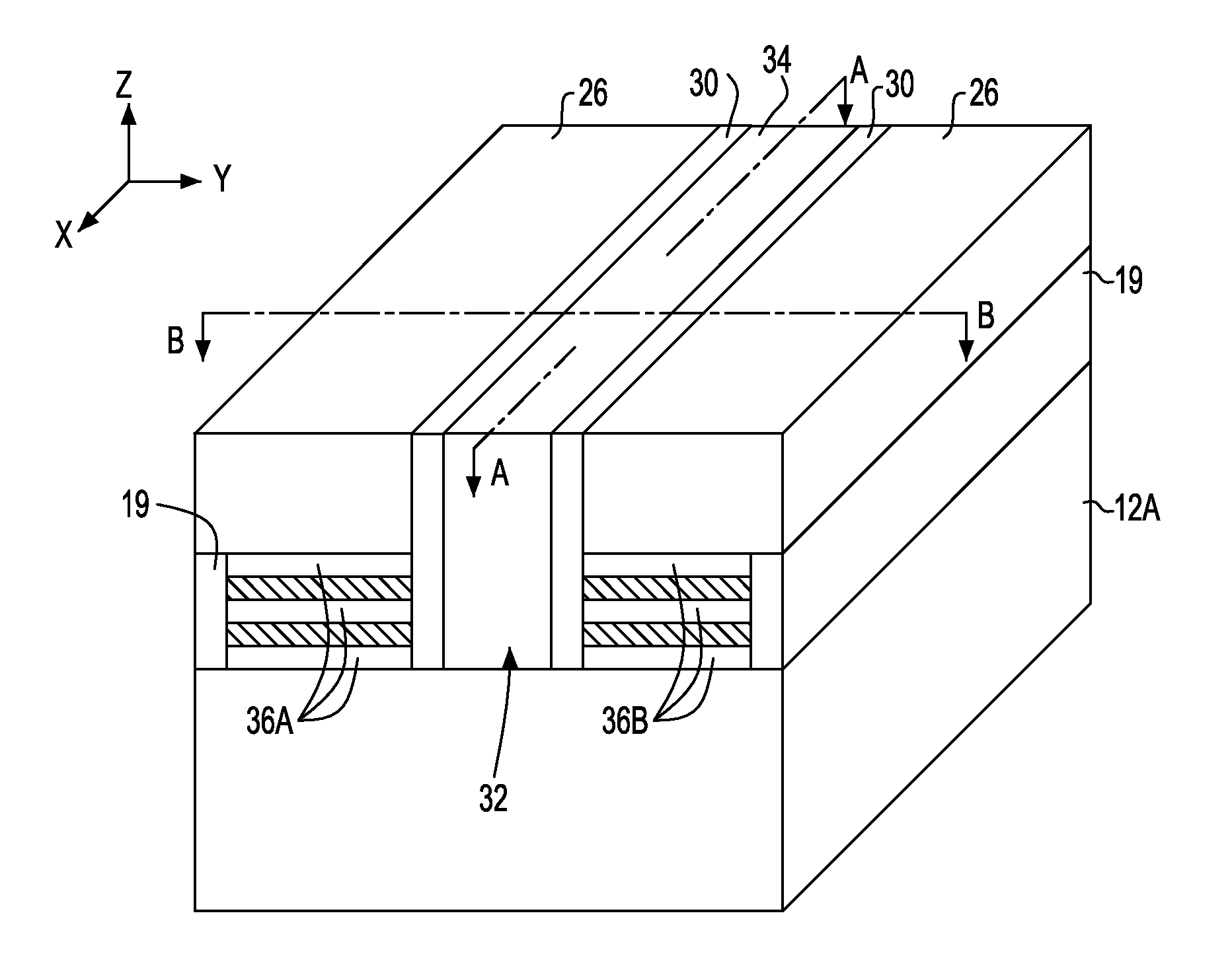
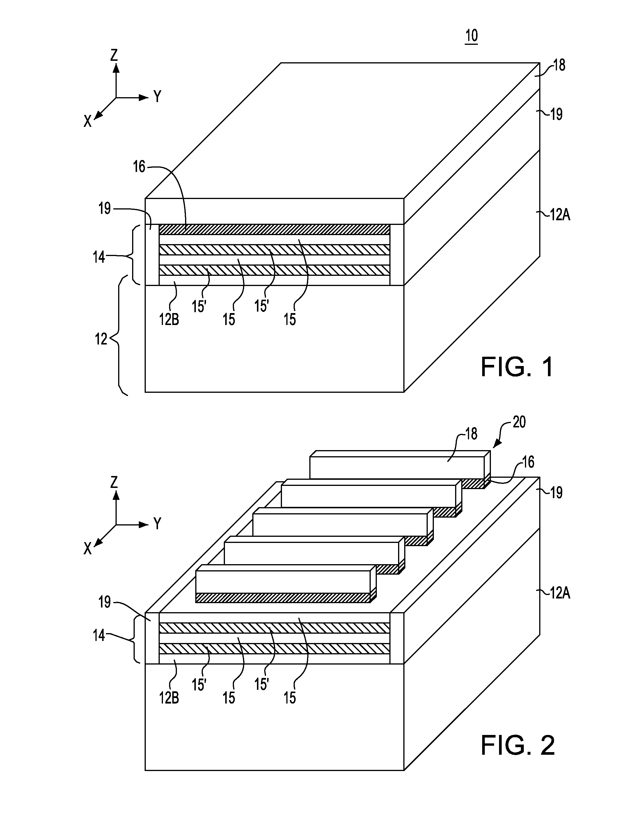
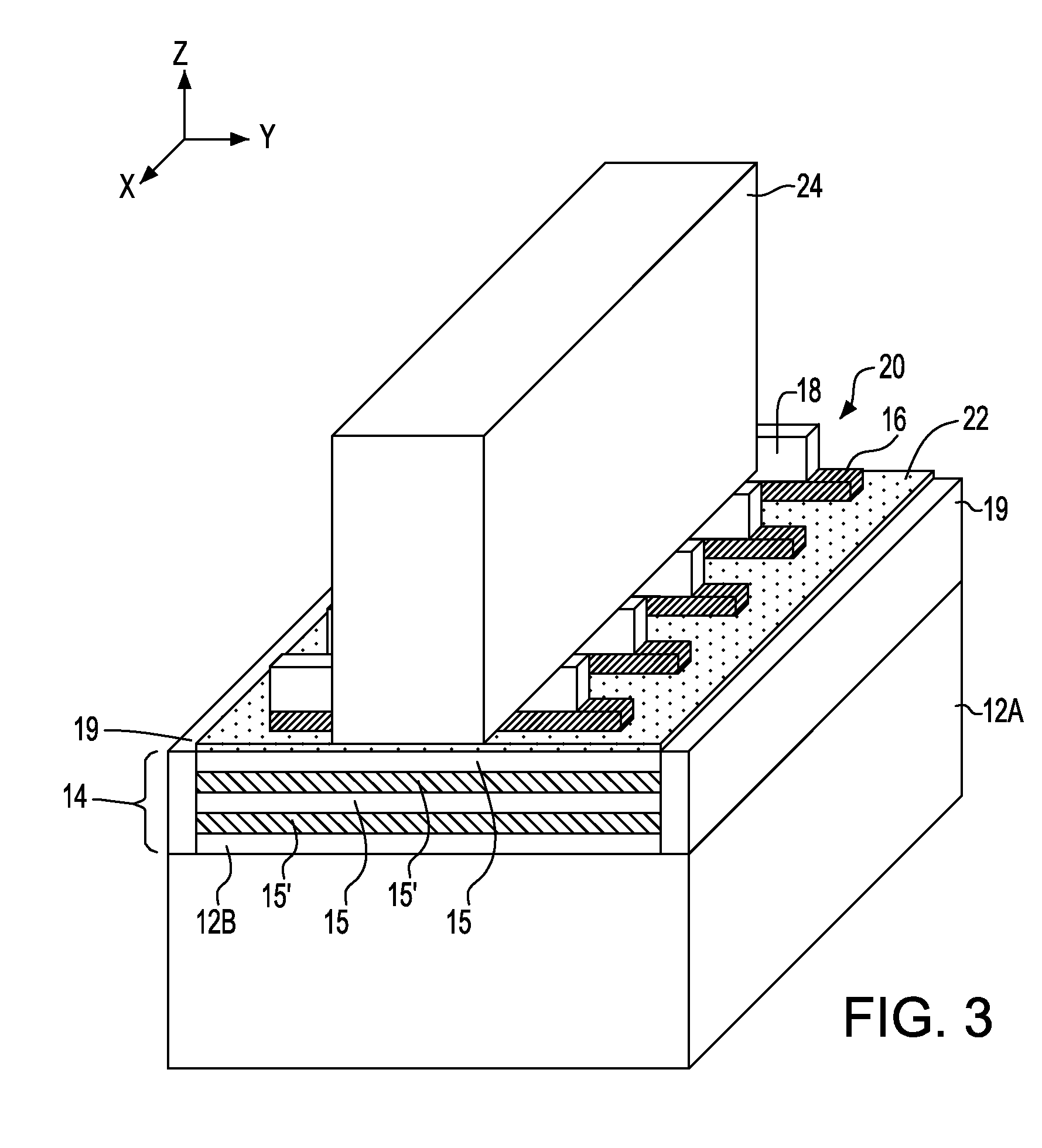
[0023]The present invention, which provides a semiconductor structure including a plurality of vertically stacked and vertically spaced apart semiconductor nanowires (e.g., nanowire mesh) and a method of fabricating such a semiconductor structure, will now be described in greater detail by referring to the following discussion and drawings that accompany the present application. It is noted that the drawings of the present application are provided for illustrative purposes only and, as such, the drawings are not drawn to scale.

[0024]In the following description, numerous specific details are set forth, such as particular structures, components, materials, dimensions, processing steps and techniques, in order to provide a thorough understanding of the present invention. However, it will be appreciated by one of ordinary skill in the art that the invention may be practiced without these specific details. In other instances, well-known structures or processing steps have not been descr...


PUM


Abstract

A semiconductor structure is provided that includes a plurality of vertically stacked and vertically spaced apart semiconductor nanowires (e.g., a semiconductor nanowire mesh) located on a surface of a substrate. One end segment of each vertically stacked and vertically spaced apart semiconductor nanowires is connected to a source region and another end segment of each vertically stacked and vertically spaced apart semiconductor nanowires is connected to a drain region. A gate region including a gate dielectric and a gate conductor abuts the plurality of vertically stacked and vertically spaced apart semiconductor nanowires, and the source regions and the drain regions are self-aligned with the gate region.

Description

CROSS REFERENCE TO RELATED APPLICATION[0001]This application is a divisional of U.S. patent application Ser. No. 12 / 371,943, filed Feb. 17, 2009 the entire content and disclosure of which is incorporated herein by reference.FIELD OF THE INVENTION[0002]The present invention relates to a semiconductor structure and a method of fabricating the same. More particularly, the present invention relates to a semiconductor structure including a plurality of vertically stacked and vertically spaced apart semiconductor nanowires and to a method of fabricating such a semiconductor structure.BACKGROUND OF THE INVENTION[0003]Due to their superior electrostatics gate-all-around nanowire channel field effect transistors (e.g., nanowire FETs) are expected to enable density scaling beyond current planar CMOS technology. In its basic form, a nanowire FET includes a source, a drain and one or more nanowire channels between the source and the drain. A gate electrode, which wraps around the one or more na...

Claims


Application Information

Patent Timeline
Patent Type & Authority Applications(United States)
IPC IPC(8): H01L21/336
CPCB82Y10/00H01L29/775H01L29/0673H01L29/42392H01L29/66545H01L29/66772H01L29/66795H01L29/785H01L29/78696Y10S977/742Y10S977/762Y10S977/938Y10S977/72B82Y40/00H01L29/66439H01L29/0665
Inventor BEDELL, STEPHEN W.CHANG, JOSEPHINE B.CHANG, PAULGUILLORN, MICHAEL A.SLEIGHT, JEFFREY W.
Owner GLOBALFOUNDRIES U S INC
Why Eureka
Try Eureka