Method to Improve Nucleation of Materials on Graphene and Carbon Nanotubes

a technology of carbon nanotubes and materials, applied in the direction of semiconductor devices, electrical equipment, transistors, etc., can solve the problems of difficult nucleation of high-k dielectric materials on carbon-based materials, difficult to uniformly coat a thin layer of any material onto the carbon surface, etc., to achieve the effect of facilitating nucleation

Active Publication Date: 2010-12-02
GLOBALFOUNDRIES US INC
View PDF17 Cites 30 Cited by
  • Summary
  • Abstract
  • Description
  • Claims
  • Application Information

AI Technical Summary

Benefits of technology

[0007]The present invention provides techniques for forming a thin coating of a material on a carbon-based material. In one aspect of the invention, a method for forming a thin coating on a surface of a carbon-based material is provided. The method includes the following steps. An ultra thin silicon nucleation layer is deposited to a thickness of from about two angstroms to about 10 angstroms on at least a portion of the surface of the carbon-based material to facilitate nucleation of the coating on the surface of the carbon-based material. The thin coating is deposited to a thickness of from about two angstroms to about 100 angstroms over the ultra thin silicon layer to form the thin coating on the surface of the carbon-based material.

Problems solved by technology

However, nucleation of high-k dielectrics on carbon-based materials such as graphene is problematic since bonding of the dielectric occurs by electrostatic forces.
The inertness makes it almost impossible to uniformly coat a thin layer of any material onto the carbon surface.
While a uniform coating can eventually be achieved by adding more of the material, depositing enough material to gain complete coverage results in a layer that is too thick for some applications.
This technique, however, shows degraded device performance due to low electron mobility.

Method used


Image

  • Method to Improve Nucleation of Materials on Graphene and Carbon Nanotubes
  • Method to Improve Nucleation of Materials on Graphene and Carbon Nanotubes
  • Method to Improve Nucleation of Materials on Graphene and Carbon Nanotubes

Examples


Embodiment Construction

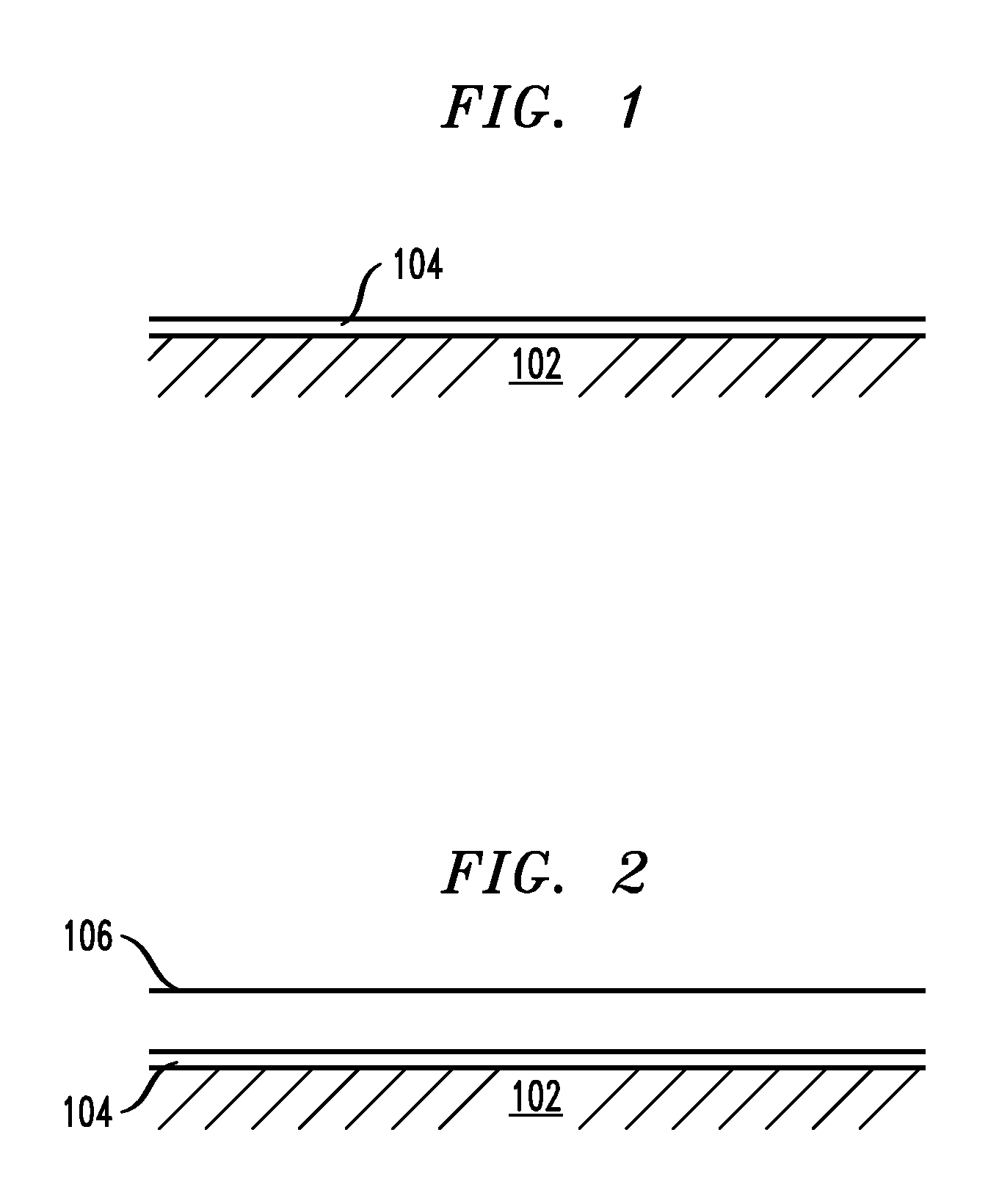
[0024]The present teachings address the above-described problems associated with thin coating chemically inert carbon-based materials. Examples of carbon-based materials as they are described herein include, but are not limited to, graphene, carbon nanotubes and carbon fibers. Advantageously, it has been determined by way of the present teachings that an ultra thin silicon nucleation layer on the surface of the carbon-based material can facilitate nucleation of the coating to achieve complete coverage of the surface, without affecting the electrical properties of the carbon-based material. By way of example only, FIGS. 1 and 2 are cross-sectional diagrams illustrating an exemplary methodology for forming a thin coating on a surface of a carbon-based material. As shown in FIG. 1, an ultra thin silicon nucleation layer 104 is deposited on a surface of carbon-based material 102. Silicon layer 104 may or may not be a continuous layer, i.e., silicon layer 104 does not have to fully cover...


PUM

PropertyMeasurementUnit
thicknessaaaaaaaaaa
thicknessaaaaaaaaaa
thicknessaaaaaaaaaa

Abstract

Techniques for forming a thin coating of a material on a carbon-based material are provided. In one aspect, a method for forming a thin coating on a surface of a carbon-based material is provided. The method includes the following steps. An ultra thin silicon nucleation layer is deposited to a thickness of from about two angstroms to about 10 angstroms on at least a portion of the surface of the carbon-based material to facilitate nucleation of the coating on the surface of the carbon-based material. The thin coating is deposited to a thickness of from about two angstroms to about 100 angstroms over the ultra thin silicon layer to form the thin coating on the surface of the carbon-based material.

Description

STATEMENT OF GOVERNMENT RIGHTS[0001]This invention was made with Government support under Contract number FA8650-08-C-7838 awarded by (DARPA) Defense Advanced Research Projects Agency. The Government has certain rights in this invention.FIELD OF THE INVENTION[0002]The present invention relates to carbon-based materials, and more particularly, to techniques for forming a thin coating of a material, such as a high-k dielectric, on a carbon-based material, such as graphene.BACKGROUND OF THE INVENTION[0003]Graphene, a one carbon atom thick material, has a very high carrier mobility, making it suitable for use in high speed, high performance electronic devices. Current trends towards feature size scaling generally involve use of a high-k dielectric in these scaled graphene-based devices.[0004]However, nucleation of high-k dielectrics on carbon-based materials such as graphene is problematic since bonding of the dielectric occurs by electrostatic forces. Specifically, carbon-based materia...

Claims


Application Information

Patent Timeline
Patent Type & Authority Applications(United States)
IPC IPC(8): H01L29/786H01L21/20H01L21/336H01L29/04
CPCH01L21/02376H01L21/02532H01L21/0262H01L29/78687H01L29/66742H01L29/78684H01L21/02664
Inventor BABICH, KATHERINACALLEGARI, ALESSANDROCHEN, ZHIHONGKIEWRA, EDWARDSUN, YANNING
Owner GLOBALFOUNDRIES US INC
Why Eureka
Try Eureka