Display device and method for manufacturing the same

a technology of display device and liquid crystal display panel, which is applied in the direction of lamination ancillary operations, instruments, chemistry apparatus and processes, etc., can solve the problems of reducing the size of the device, affecting the reliability of the liquid crystal display device, and reducing the thickness of the two substrates. , to achieve the effect of reducing the thickness of the two substrates

Inactive Publication Date: 2010-12-09
MIYAMOTO KENJI
View PDF15 Cites 5 Cited by
  • Summary
  • Abstract
  • Description
  • Claims
  • Application Information

AI Technical Summary

Benefits of technology

[0018]In light of the above-described problems, the present invention has been achieved. An object of the present invention is to slim down the display device through simple manufacturing steps with reduction in production cost and improvement in yield.
[0034]A method for manufacturing a display device according to the present invention includes the steps of: bonding a first substrate including a glass substrate and a second substrate including a glass substrate to each other and forming a display medium layer between the first substrate and the second substrate, the glass substrate of the second substrate having a thickness different from that of the glass substrate of the first substrate and being etched by an etching solution at the same rate as the glass substrate of the first substrate; and immersing the first substrate and the second substrate bonded to each other in an etching solution such that each of the glass substrates is thinned down.
[0037]A first substrate and a second substrate as components of a display device include glass substrates, respectively. If the etch rates of the glass substrates in an etching solution are varied, the glass substrates are etched by different thicknesses even if they are immersed in the etching solution for the same period of time. Therefore, if the glass substrates have the same thickness before they are subjected to etching, the total thickness of the first and second substrates is reduced and the glass substrates are varied in thickness after the etching. The glass substrates preferably have the same thickness before etching such that the glass substrates are easily handled in the manufacture line.
[0038]When a flexible printed substrate is press-mounted on the substrate, the substrate needs to have certain mechanical strength. Therefore, the glass substrate of the first substrate is made thicker than the glass substrate of the second substrate such that the glass substrate of the first substrate has higher mechanical strength than the glass substrate of the second substrate. Specifically, the total thickness of the first and second substrates is reduced while ensuring the strength of the first substrate, thereby permitting the flexible printed substrate to be mounted on the first substrate.
[0039]On the first substrate, a driver including an element made of low-temperature polysilicon or CG silicon is formed. Therefore, the thickness of the display device is further reduced.
[0041]If the glass substrate of the first substrate and the glass substrate of the second substrate have different initial thicknesses and the same etch rate, the total thickness of the two substrates is reduced and one of the substrates is made thinner than the other by immersing the two substrates in an etching solution for the same period of time.

Problems solved by technology

In particular when the final size of a device is required to be small, the slimming down of the liquid crystal display panel 100 as one of the components thereof is a very important issue.
Therefore, even though the other components are downsized, dramatic size reduction of the device cannot be expected unless the size of the liquid crystal display panel 100 is reduced.
As a result, the strength of the glass substrates 101 and 102 decreases, thereby inevitably impairing the reliability of the liquid crystal display device (resistance against vibration and drop).
If the thicknesses a and b of the glass substrates 101 and 102 are reduced to as small as about 0.3 mm, it would be difficult to handle the glass substrates 101 and 102 during the manufacture of the liquid crystal display device and problems may arise in terms of cost and yield.
In reality, however, it is still difficult to handle the thin glass substrates in a usual manufacture line in terms of strength.
That is, both of the methods require several additional steps, whereby problems may arise in terms of production cost and yield.

Method used


Image

  • Display device and method for manufacturing the same
  • Display device and method for manufacturing the same
  • Display device and method for manufacturing the same

Examples


first embodiment

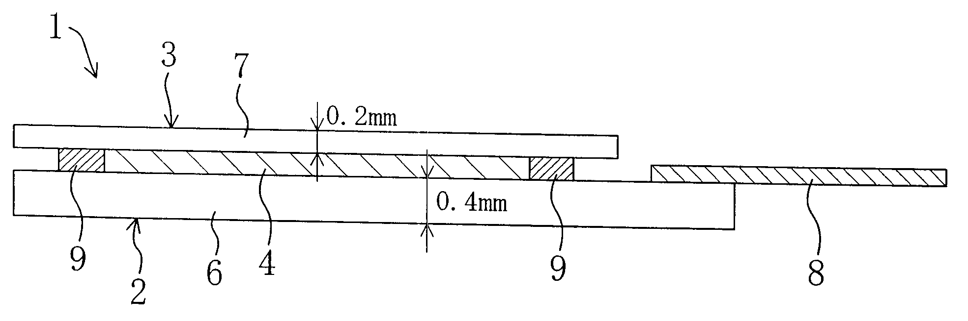
[0052]FIGS. 1 to 5 show a first embodiment of the present invention.

[0053]FIG. 1 is a sectional view schematically illustrating a liquid crystal display device 1 as a display device of the present invention. As shown in FIG. 1, the liquid crystal display device 1 includes an active matrix substrate 2 as a first substrate, a counter substrate 3 as a second substrate facing the active matrix substrate 2 and a liquid crystal layer 4 as a display medium layer provided between the substrates 2 and 3.

[0054]The active matrix substrate 2 includes a glass substrate 6 and a plurality of thin film transistors (not shown and abbreviated as TFTs) which are formed on the surface of the glass substrate 6 facing the liquid crystal layer 4. The active matrix substrate 2 further includes a plurality of pixels arranged in a matrix. The TFTs are provided on a pixel-by-pixel basis.

[0055]The thickness of the glass substrate 6 is 0.4 mm, for example. An orientation film (not shown) is formed on the surfac...

example

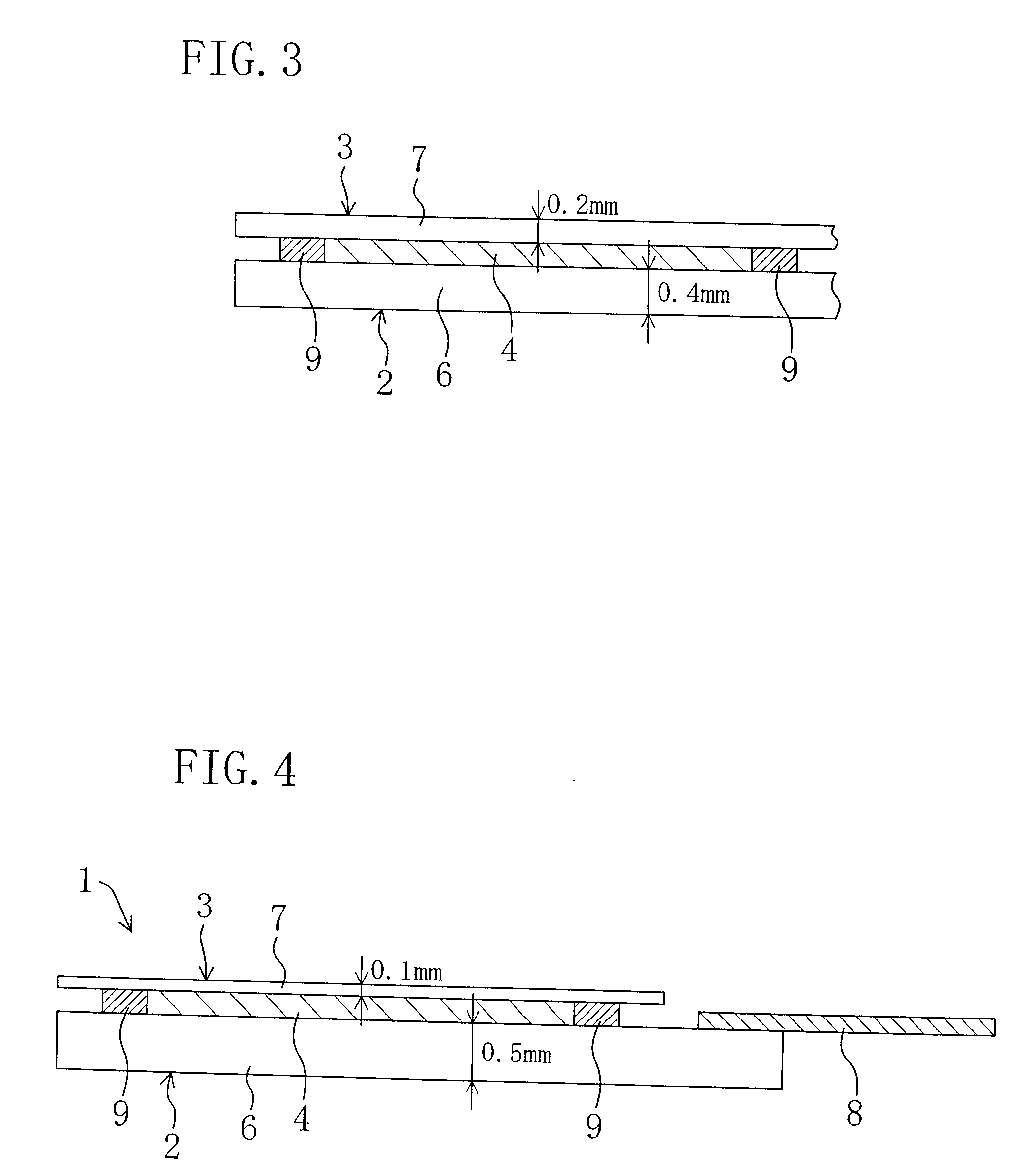
[0071]Now, an explanation of a specific example of the present invention will be provided.

[0072]A glass substrate A (AN100 manufactured by ASAHI GLASS) was used as the glass substrate 6 of the active matrix substrate 2 and a glass substrate B (1737 manufactured by Corning) was used as the glass substrate 7 of the counter substrate 3. Under certain etching conditions, the etch rate of the glass substrate A is 4.4 μm / min and that of the glass substrate B is 5.2 μm / min.

[0073]Elements such as TFTs and wires were formed on the glass substrate A and a color filter and other elements were formed on the glass substrate B. Then, the glass substrates A and B are bonded together. The bonded substrates were immersed in an etching solution containing hydrogen fluoride under the above-described conditions to etch the substrates for about 42 minutes. As shown in Table 1, the thicknesses of the glass substrates A and B after the 42-minute etching were 0.52 mm and 0.48 mm, respectively.

TABLE 1Time (...

second embodiment

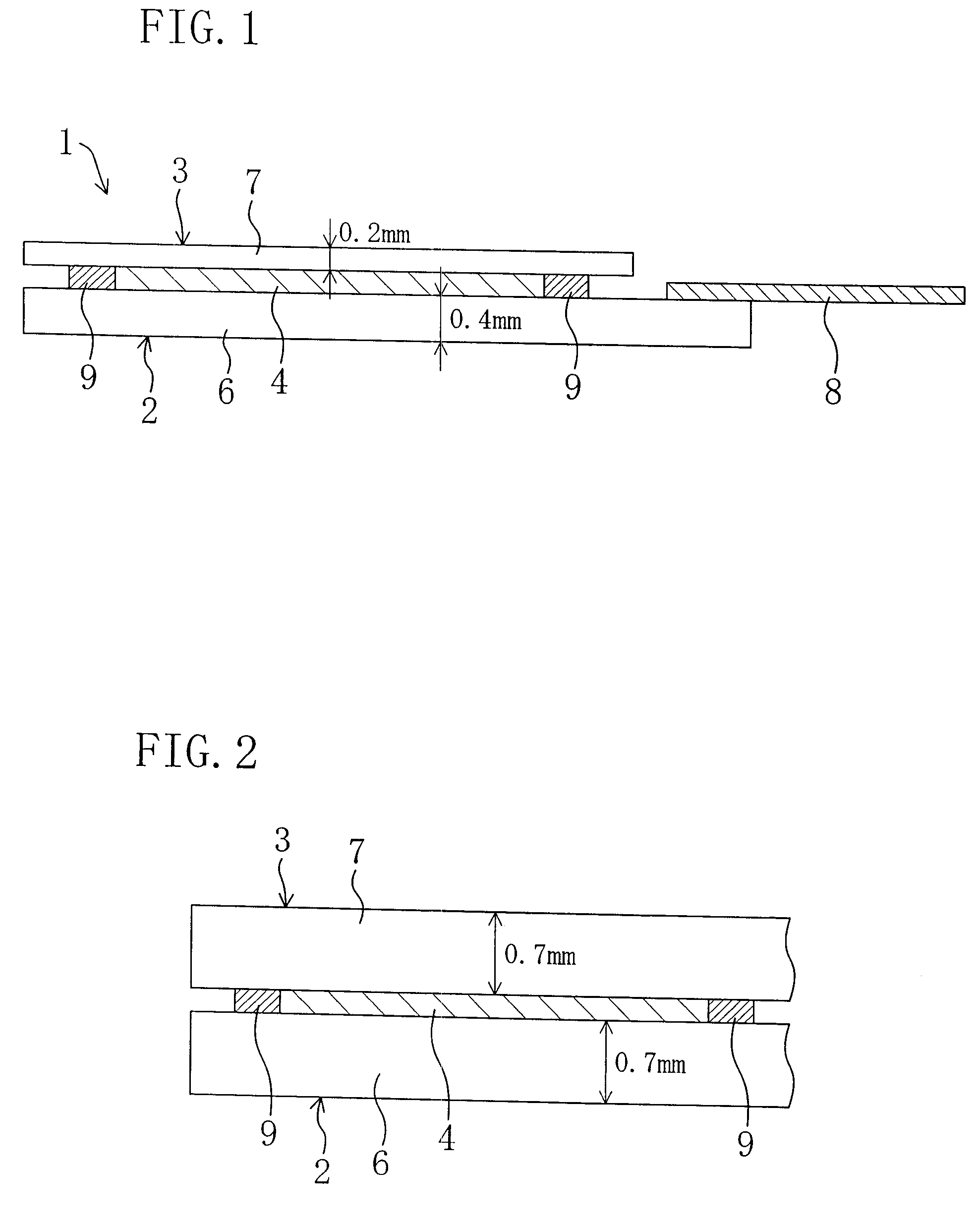
[0075]FIG. 6 shows a second embodiment of the present invention. In the following embodiments, the same components as those shown in FIGS. 1 to 4 are indicated by the same reference numerals to omit a detailed explanation.

[0076]A liquid crystal display device 1 of the present embodiment includes an active matrix substrate 2, a counter substrate 3 and a liquid crystal layer 4 as shown in FIG. 6. The active matrix substrate 2 includes a 0.5 mm thick glass substrate 6. The counter substrate 3 includes a 0.1 mm thick plastic substrate 10. In other words, the liquid crystal display device 1 includes the glass substrate 6 and the plastic substrate 10 which is provided to face the glass substrate 6 and thinner than the glass substrate 6.

[0077]In order to fabricate the liquid crystal display device 1 described above, first, in the step of bonding the substrates, a color filter (a coloring layer), TFTs, pixel electrodes, signal wires, scanning wires and a driver which are not shown in the dr...


PUM

PropertyMeasurementUnit
thicknessesaaaaaaaaaa

Abstract

A liquid crystal display device includes: an active matrix substrate including a glass substrate; a counter substrate which is arranged to face the active matrix substrate and includes a glass substrate which is thinner than the glass substrate of the active matrix substrate; and a display medium layer which is provided between the active matrix substrate and the counter substrate. The rate at which the glass substrate of the active matrix substrate is etched by an etching solution is lower than the rate at which the glass substrate of the counter substrate is etched by the etching solution.

Description

CROSS-REFERENCE TO RELATED APPLICATION[0001]This application is a Divisional of co-pending application Ser. No. 11 / 406,241 filed on Apr. 19, 2006, which claims priority to Application No. 2005-128664 filed in JP, on Apr. 26, 2005. The entire contents of all of the above applications is hereby incorporated by reference.BACKGROUND OF THE INVENTION[0002]1. Field of the Invention[0003]The present invention relates to a display device including a display medium layer provided between a pair of substrates and a method for manufacturing the same.[0004]2. Description of Related Art[0005]In recent years, there has been a growing demand for mobile devices such as cellular phones and digital video cameras. The mobile devices are provided with display devices such as liquid crystal display panels. These liquid crystal display devices are relatively medium or small in size. For example, as shown in FIG. 9, a liquid crystal display panel 100 includes a pair of glass substrates 101 and 102 and a l...

Claims


Application Information

Patent Timeline
Patent Type & Authority Applications(United States)
IPC IPC(8): B32B38/10
CPCG02F1/1333G02F2001/133368G02F2001/133302G02F1/13454G02F1/133302G02F1/133368
Inventor MIYAMOTO, KENJI
Owner MIYAMOTO KENJI
Why Eureka
Try Eureka