

Switching power supply apparatus and semiconductor device
- Summary
- Abstract
- Description
- Claims
- Application Information
AI Technical Summary
Benefits of technology
Problems solved by technology
Method used
Image

Examples
first embodiment
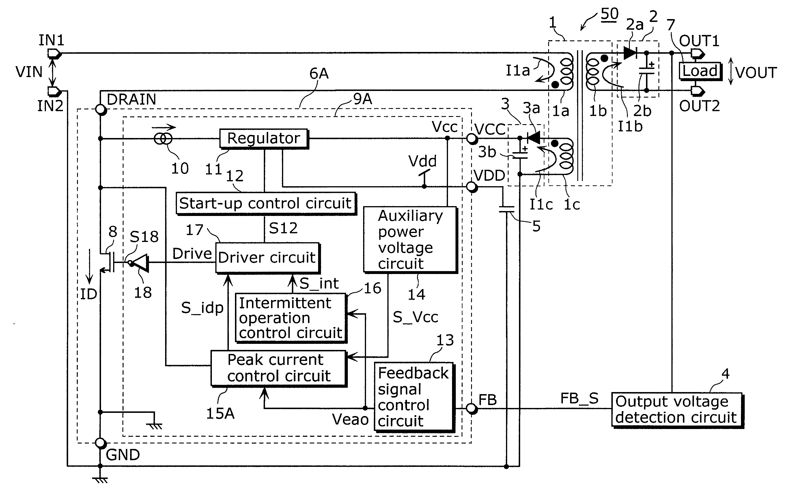
[0116]FIG. 1 is a block diagram showing an example of a configuration of a switching power supply apparatus 50 according to the first embodiment of the present invention.
[0117]The switching power supply apparatus 50 shown in FIG. 1 includes an input terminal IN1, an input terminal IN2, an output terminal OUT1, an output terminal OUT2, a transformer 1, an output voltage generation circuit 2, an auxiliary power voltage generation circuit 3, an output voltage detection circuit 4, a capacitor 5, and a semiconductor device 6A. The switching power supply apparatus 50 supplies a substantially direct-current output voltage VOUT to a load 7 connected between the output terminal OUT1 and the output terminal OUT2 based on a substantially direct-current input voltage VIN provided between the input terminal IN1 and the input terminal IN2.
[0118]The semiconductor device 6A includes a switching device 8, a drain terminal DRAIN, an auxiliary power voltage input terminal VCC, an internal circuit powe...
second embodiment
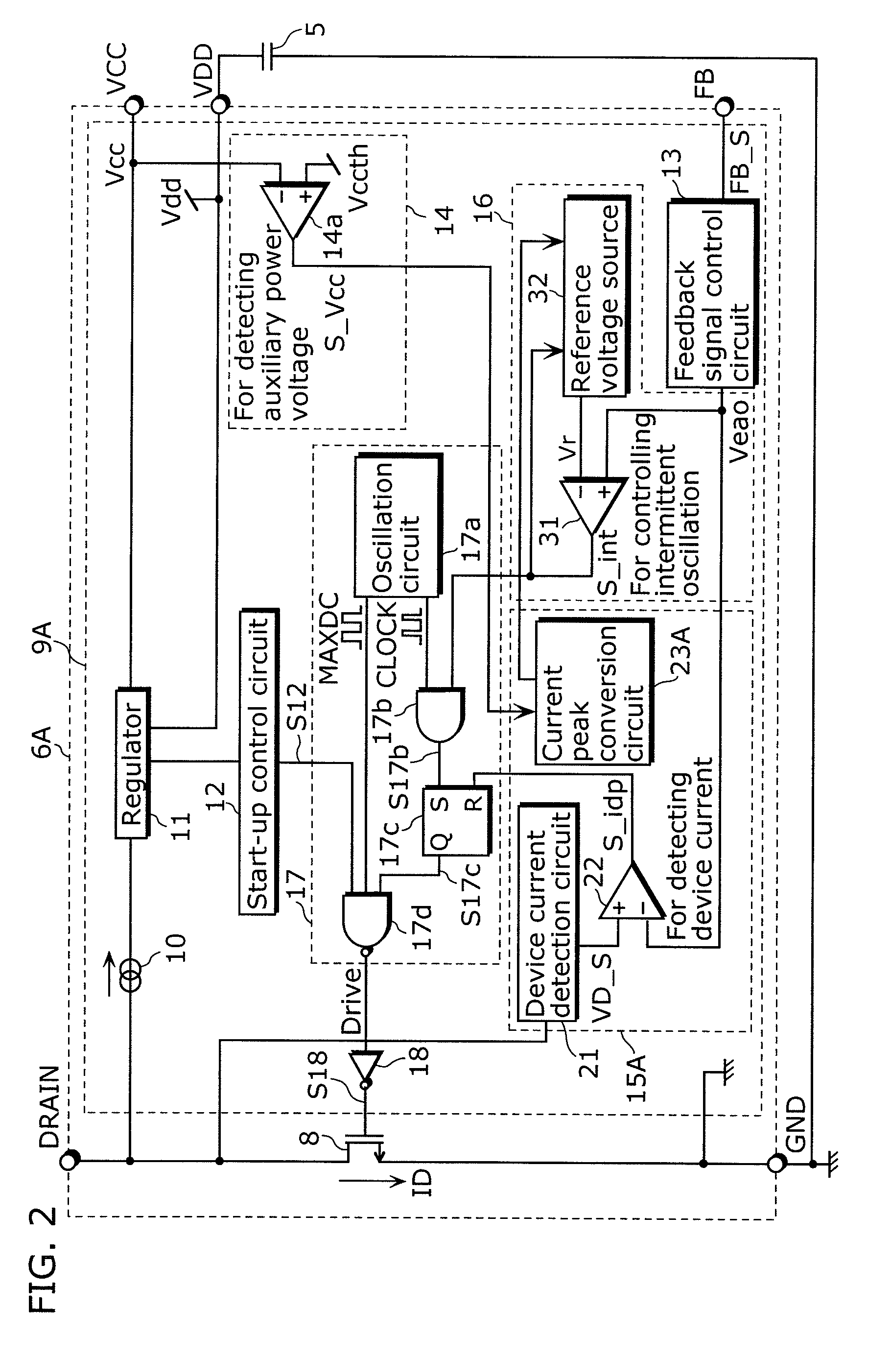
[0235]The switching power supply apparatus 50 according to the second embodiment of the present invention is a variation of the above-described switching power supply apparatus 50 according to the first embodiment and is different from the switching power supply apparatus 50 according to the first embodiment in the configuration for lowering the current peak IDP in the auxiliary power voltage decrease mode. To be specific, the switching power supply apparatus 50 according to the second embodiment lowers the current peak IDP in the auxiliary power voltage decrease mode by decreasing the feedback control signal Veao_S which is inputted to the comparison circuit for detecting device current 22 in the auxiliary power voltage decrease mode.
[0236]The following explanation for the second embodiment will focus on the differences from the first embodiment. The other configurations, operations, and effects will not be explained since they are the same as or like those in the first embodiment....
third embodiment
[0260]The switching power supply apparatus 50 according to the third embodiment of the present invention is a variation of the above-described switching power supply apparatus 50 according to the first embodiment and is different from the switching power supply apparatus 50 according to the first embodiment in the configuration for lowering the current peak IDP in the auxiliary power voltage decrease mode. To be specific, the switching power supply apparatus 50 according to the third embodiment lowers the current peak IDP in the auxiliary power voltage decrease mode by increasing the device current detection signal VD_S which is inputted to the comparison circuit for detecting device current 22 in the auxiliary power voltage decrease mode.
[0261]The following explanation for the third embodiment will focus on the differences from the first and second embodiments. The other configurations, operations, and effects will not be explained since they are the same or alike as those in the f...
PUM
 Abstract
Description
Claims
Application Information