

Method of manufacturing wiring substrate
a manufacturing method and wiring technology, applied in the manufacture of printed circuits, printed circuit aspects, basic electric elements, etc., can solve the problems of deterioration in the reliability of the connection portions, electrical characteristics or reliability of the whole of the semiconductor package, etc., and achieve the effect of improving the reliability of the wiring substra
- Summary
- Abstract
- Description
- Claims
- Application Information
AI Technical Summary
Benefits of technology
Problems solved by technology
Method used
Image

Examples
first embodiment
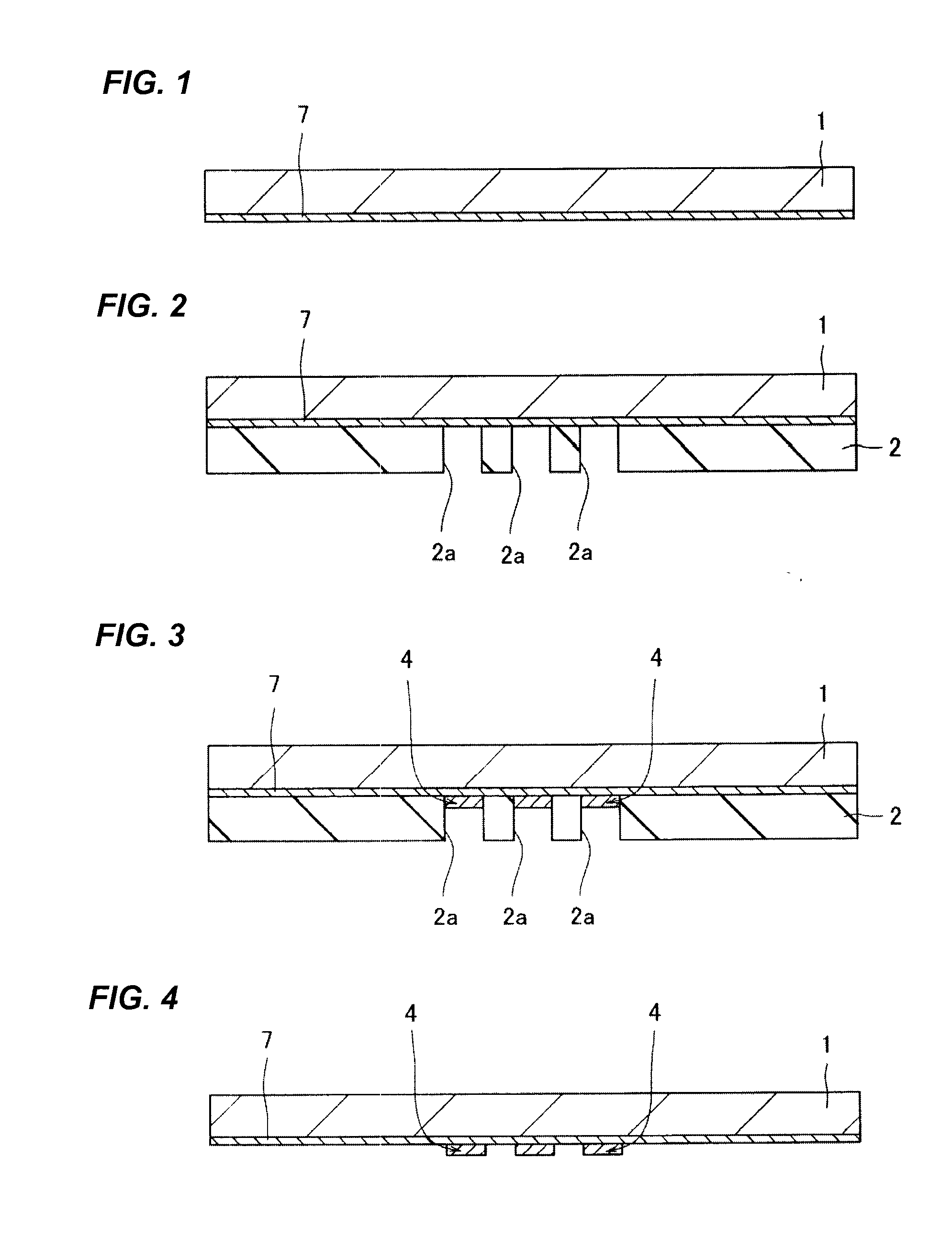
[0086]A method of manufacturing a semiconductor package of this embodiment will be described with reference to the drawings. First, as shown in FIG. 1, a conductive feeding layer 7 of a material different from a support plate 1 is formed on the support plate 1. The support plate 1 is, for example, a Cu (copper) foil having a thickness of about 500 μm. The feeding layer 7 is, for example, an Ni (nickel) plated film which is formed by a plating method to have a thickness of about 1 to 5 μm. For the support plate 1, various metal foils other than a Cu foil may be used.
[0087]The feeding layer 7 may be an Al (aluminum) film or the like insofar as the film is conductive, and may be formed by a sputtering method. In this embodiment, because an electrolytic plating method is carried out using the feeding layer 7 as a plating conduction plate in a subsequent step, the feeding layer 7 is preferably conductive. The support plate 1 preferably has a thickness such that no warpage occurs in the s...
second embodiment
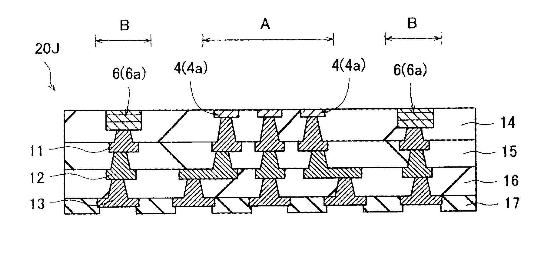
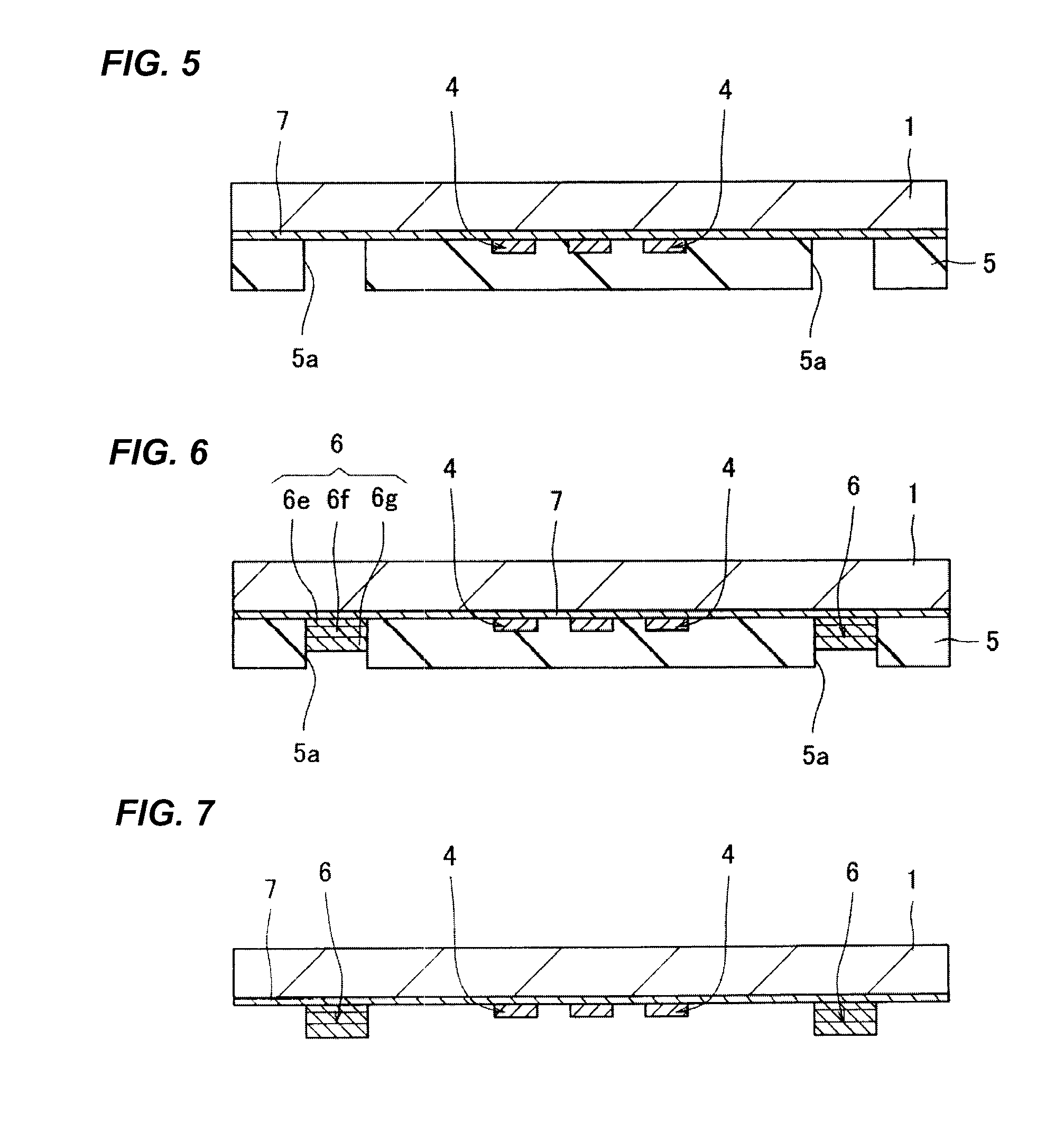
[0120]In the first embodiment, as shown in FIG. 10, a case has been described where a Cu plated film is exposed at the surfaces of the electrode pads 4a connected to the semiconductor chip 21 in the region A, and an Au plated film is exposed at the surfaces of the electrode pads 6a connected to the lid 23 in the region B, such that the materials for the exposed surfaces are different between the electrode pads. In this embodiment, as shown in FIG. 17, a case will be described where an Au plated film is exposed at the surfaces of electrode pads 6a connected to a semiconductor chip 21 in a region A, and a Cu plated film is exposed at the surfaces of electrode pads 4a connected to a lid 23 in a region B. Overlapping description between the foregoing embodiment and this embodiment may be omitted.
[0121]A method of manufacturing a semiconductor package of this embodiment will be described with reference to the drawings. After the manufacturing process of the first embodiment described wit...
third embodiment
[0131]In the first embodiment, as shown in FIG. 10, a case has been described where, in the wiring substrate 20J in which the materials for the exposed surfaces differ between the electrode pads, a Cu plated film is exposed as the electrode pads 4a connected to the semiconductor chip 21 in the region A, and an Au plated film is exposed as the electrode pads 6a connected to the lid 23 in the region B. In this embodiment, as shown in FIG. 27, a case will be described where, in a region A at the central portion of a wiring substrate 20A, the exposed surfaces of electrode pads 4a are flush with the bottom of concave portions 18 formed in an insulating interlayer 14, and in a region B at the peripheral portion of the wiring substrate 20A, the exposed surfaces of electrode pads 6a are flush with the surface of the insulating interlayer 14. Overlapping description between the foregoing embodiment and this embodiment may be omitted.
[0132]A method of manufacturing a semiconductor package of ...
PUM
| Property | Measurement | Unit |
|---|---|---|
| thickness | aaaaa | aaaaa |
| thickness | aaaaa | aaaaa |
| thickness | aaaaa | aaaaa |
Abstract
Description
Claims
Application Information