Power control circuit

a power control circuit and logic level technology, applied in the direction of pulse counters, amplifiers, high frequency amplifiers, etc., can solve the problems of additional d.c. bias current disadvantageous in portable applications, power down signal at logic level of digvdd may not be sufficient to correctly implement the power down function,

Inactive Publication Date: 2010-12-16
FUTURE WAVES UK
View PDF4 Cites 1 Cited by
  • Summary
  • Abstract
  • Description
  • Claims
  • Application Information

AI Technical Summary

Benefits of technology

[0028]The apparatus may comprise a delay means, such as delay circuitry, to output a signal only if an input signal is maintained for a pre-determined length of time. Thus, the effect of extraneous signals such as spikes, may be mitigated. The apparatus may be arranged so that the delay means operates on any of the input signals mentioned herein, and in particular on the power-down or power-up signals mentioned herein.

Problems solved by technology

For the various analogue circuits 15 operating directly from RFVDD, a power down signal at a logic level of DIGVDD may not be sufficient to correctly implement the power down function.
This additional d.c. bias current may be disadvantageous in portable applications which operate from a battery.
At the same time, problems may also occur if the external controller 12 sends a command to power off the on-chip voltage regulator 18 which generates the digital supply voltage, DIGVDD.
Secondly, since the digital supply voltage is removed, the serial interface 19 will no longer work and it will not be possible to power up the chip 11 again by sending commands via this interface 19.
In addition, in system-on-chip designs, external pins are typically limited and there may not be one pin spare to implement this regulator power down function.
If the regulator power down function is not provided, then in standby mode the regulators generating the digital supply voltage will remain on, which will result in wasted power.

Method used


Image

  • Power control circuit
  • Power control circuit
  • Power control circuit

Examples


Embodiment Construction

[0039]An apparatus for processing signals is disclosed. In the following description, a number of specific details are presented in order to provide a thorough understanding of embodiments of the present invention. It will be apparent, however, to a person skilled in the art that these specific details need not be employed to practice the present invention.

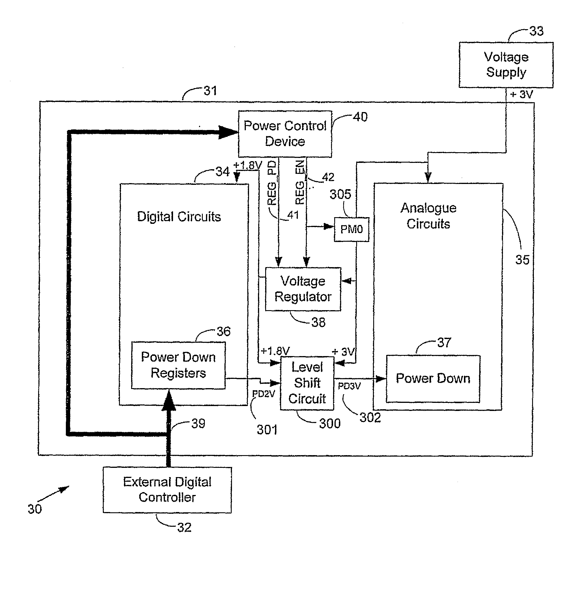
[0040]FIG. 3 shows a mixed signal chip 31 comprising a power control device 40 according to an embodiment of the present invention. A feature of the present invention is that an external controller 32 can put the entire chip 31 into a total power-down state. The external controller 32 comprises, in this example, a microcontroller, but could include a digital signal processor (DSP), an application specific integrated circuit (ASIC) device or any other device capable of processing signals and sending commands. In order to power down the mixed signal chip 31 and the on-chip voltage regulator 38, an appropriate command must be sent vi...


PUM


Abstract

Apparatus for controlling an integrated circuit comprises a power control device for controlling the power to at least part of the integrated circuit, the power control device is connected to a first input, for receiving a power-down signal, and a second input, for receiving a power-up signal, the power control device is adapted to power-up the at least part of the integrated circuit if a power-up signal is received at the second input when the at least part of the integrated circuit is in a powered-down state, and the power control device is further adapted to maintain the at least part of the integrated circuit in the powered-up state regardless of any signal received at the second input when the at least part of the integrated circuit is in a powered-up state, the apparatus is arranged so that the second input is also connected to a component of the integrated circuit and the apparatus comprising means for sending a signal to the component of the integrated circuit via the second input when the at least part of the integrated circuit is in the powered-up state.

Description

CROSS-REFERENCE TO RELATED APPLICATIONS[0001]This national stage application claims the benefit under 35 U.S.C. §371 of International Application No. PCT / GB2007 / 050017 filed on Jan. 15, 2007, entitled POWER CONTROL CIRCUIT, which takes its priority from U.S. Provisional application Ser. No. 60 / 761,363 filed on Jan. 24, 2006 and also takes its priority from GB Application No. 0604386.3 filed on Mar. 6, 2006, and all of whose entire disclosures are incorporated by reference herein.FIELD OF THE INVENTION[0002]The present invention generally relates to a power control circuit for use in an integrated circuit (IC) chip.BACKGROUND OF THE INVENTION[0003]Referring to FIG. 1, a mixed-signal IC chip 11 combines both analogue 15 and digital 14 circuits on a single semiconductor die. Mixed-signal ICs 11 may operate from a single voltage supply 13 (herein referred to as RFVDD) typically of 3 volts (V), with analogue circuits 15 generally powered directly from this voltage. However, a lower suppl...

Claims


Application Information

Patent Timeline
Patent Type & Authority Applications(United States)
IPC IPC(8): H03K17/00
CPCG06F1/3203G06F1/3287G11C5/144G11C5/147H03F3/189H03F3/45188Y02D50/20H03F2200/372H03F2200/489H03F2200/492H03K23/544Y02D10/171H03F2200/294Y02D10/00Y02D30/50G06F1/26G11C5/14
Inventor BURDETT, ALISON
Owner FUTURE WAVES UK
Why Eureka
Try Eureka