Display with pixel arrangement

a technology of pixel groups and displays, applied in the field of displays having pixel groups, can solve the problems of inability to perform critical functions, direct conflict with the display market's demand for high-resolution displays, and impracticality of arrangement for most flat-panel display applications, so as to reduce the current density of emitters, reduce artifacts in displayed images, and increase the light-emitting area of emissive displays

Active Publication Date: 2010-12-16
GLOBAL OLED TECH
View PDF20 Cites 223 Cited by
  • Summary
  • Abstract
  • Description
  • Claims
  • Application Information

AI Technical Summary

Benefits of technology

[0015]b) one or more electrical elements arranged within the gutter, each subpixel being connected to one of the one or more electrical elements, wherein the gutter dimension is greater than the inter-pixel separation, so that artifacts in a displayed image are reduced.
[0016]By arranging the organization of the pixels, a more efficient pixel design is provided that increases the light-emitting area of an emissive display and thereby reduces current density of the emitters. This advantage is obtained while reducing the visibility of any artifacts that arise as a result of such arrangements and thereby maintaining image quality.

Problems solved by technology

However, when these electrical elements are too small, they are unable to perform critical functions, such as distributing power among the subpixels within the display area.
This constraint directly conflicts with the display market's demand for high-resolution displays.
However, this disclosure does not discuss or describe the routing of electrical elements within this random array.
The requirement for the electrical elements and the light-emitting portion of the subpixels to share space within the display area, as well as manufacturing yield and performance considerations which dictate the need for the electrical elements to nearly follow a regular grid, makes such an arrangement impractical for most flat-panel display applications.

Method used


Image

  • Display with pixel arrangement
  • Display with pixel arrangement
  • Display with pixel arrangement

Examples


Embodiment Construction

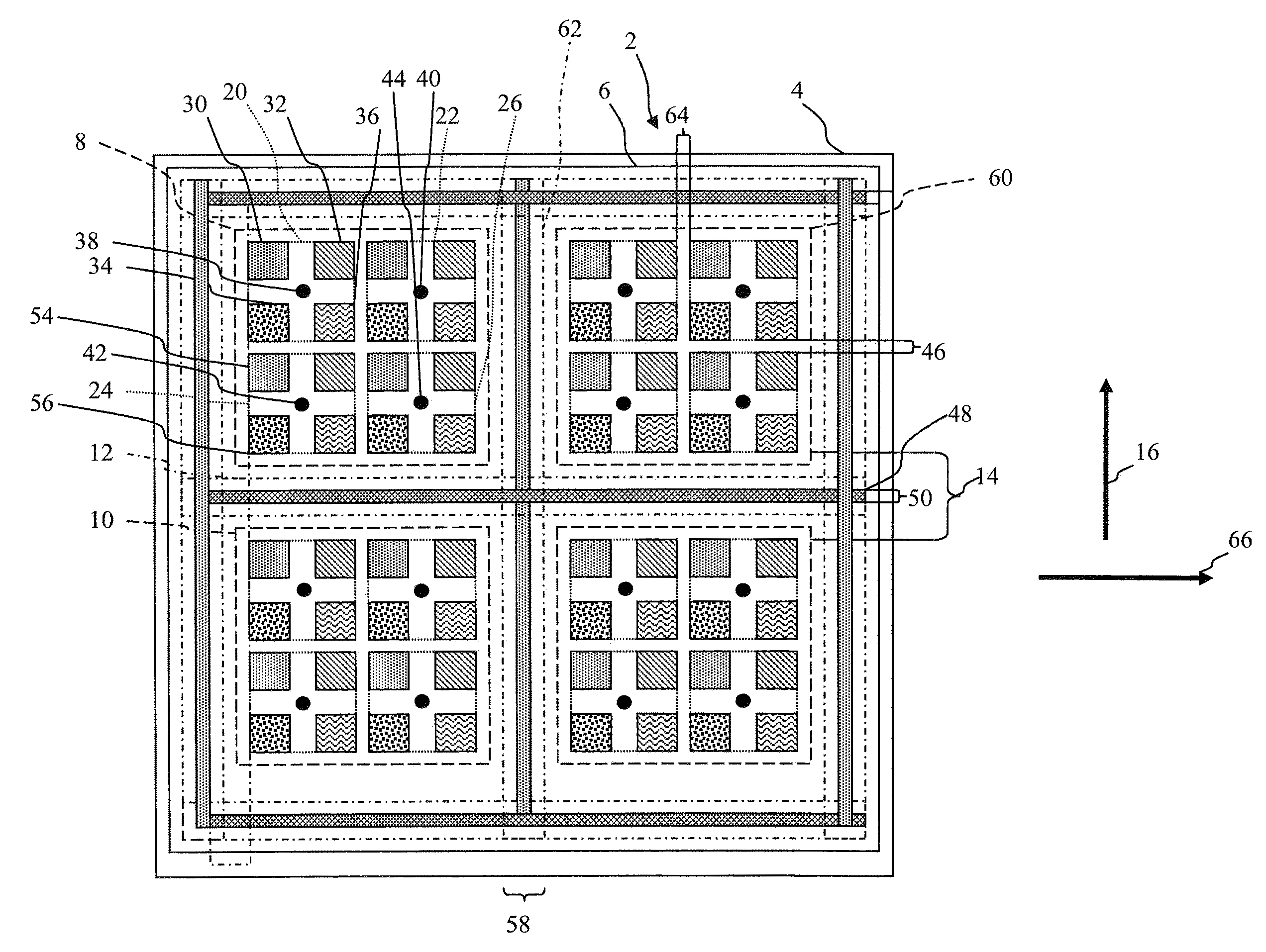
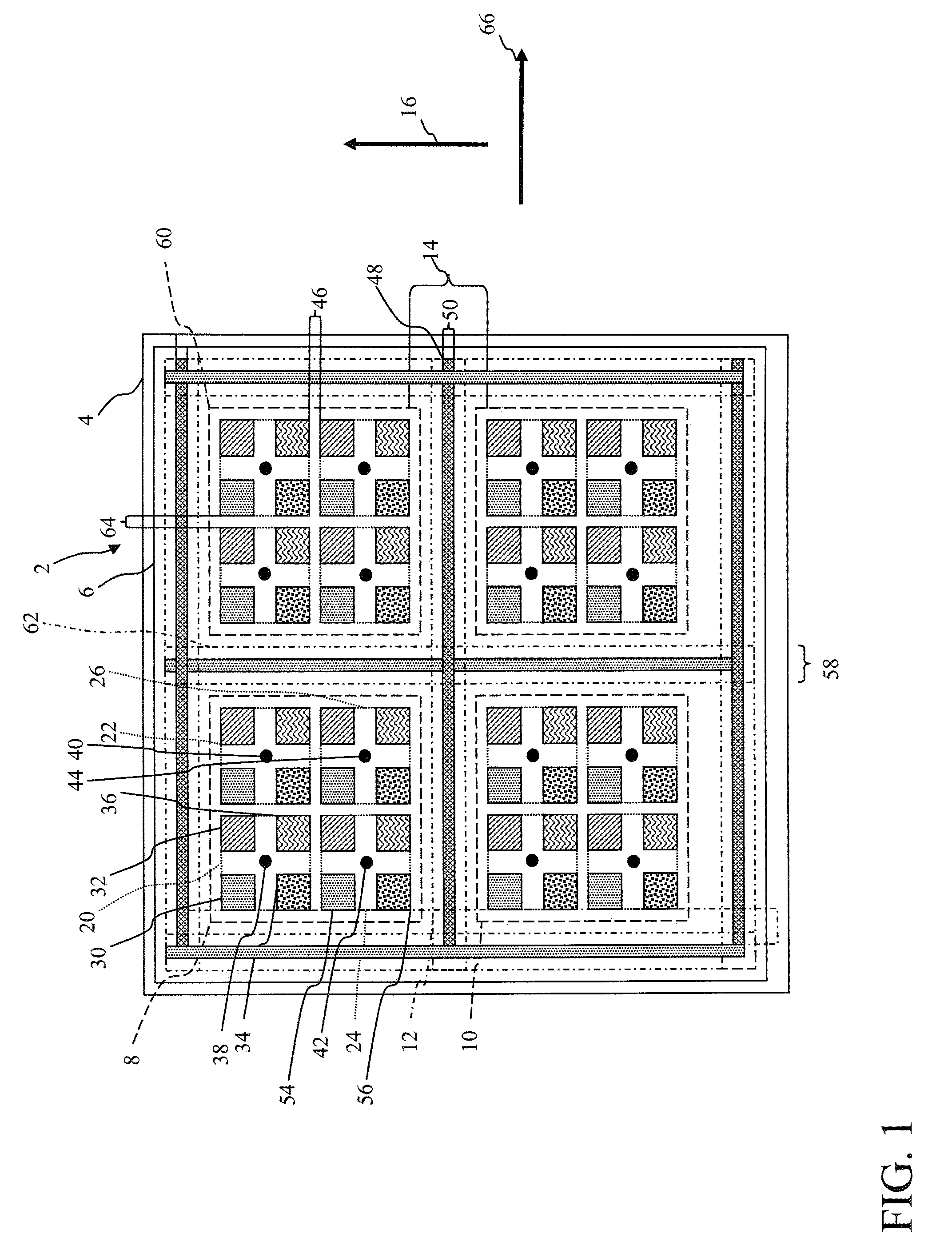
[0026]The present invention provides a display having an improved fill factor, providing reduced current densities in an electro-luminescent (EL) display with reduced image artifacts. An example of a portion of such a display 2 is shown in FIG. 1. As shown, this display 2 includes a substrate 4 and a display area 6 containing pixels, wherein the display area 6 is less than the size or area of the substrate 4. The display area 6 includes a first and a second non-overlapping pixel group 8, 10 and a gutter 12 located between the first and the second non-overlapping pixel group 8, 10. This gutter 12 contains electrical elements for providing power or control signals to multiple rows or columns of pixels as will be further explained. This gutter 12 has a dimension 14 in a first direction, indicated by arrow 16 separating the first and second pixel groups 8, 10. The gutter dimension 14 is measured to include the space between pixels as shown in FIG. 1. In a typical arrangement, an edge of...


PUM


Abstract

A display, including a substrate having a display area including first and second non-overlapping pixel groups and a gutter located between the first and second pixel groups, the gutter having a dimension in a first direction separating the first and second pixel groups, and each pixel group includes a plurality of pixels, each pixel having three or more differently colored sub-pixels; and wherein the pixel centers of the pixels in each pixel group are arranged in a regular two-dimensional array having one dimension parallel to the first direction, and wherein the pixels within a pixel group are separated by an inter-pixel separation in the first direction; and one or more electrical elements arranged within the gutter, each subpixel being connected to one of the one or more electrical elements, wherein the gutter dimension is greater than the inter-pixel separation, so that artifacts in a displayed image are reduced.

Description

CROSS REFERENCE TO RELATED APPLICATIONS[0001]Reference is made to commonly-assigned U.S. Patent Application Ser. No. 12 / 191,478 filed Aug. 14, 2008 entitled “OLED DEVICE WITH EMBEDDED CHIP DRIVING” to Dustin L. Winters et al., the disclosure of which is incorporated herein.FIELD OF THE INVENTION[0002]The present invention relates to a display having pixel groups, and more particularly to the organization of such groups on the display to thereby reduce current density of organic electroluminescent emitters while maintaining image quality.BACKGROUND OF THE INVENTION[0003]Flat-panel displays based upon many technologies, including liquid crystal, plasma, electro-luminescent (EL) display technologies, are well known in the art. Generally, these displays include a substrate having a display area. Individual light-emitting elements or subpixels are then arranged within this display area. Typically, a fixed and repeated distance in both the horizontal and vertical directions separates the ...

Claims


Application Information

Patent Timeline
Patent Type & Authority Applications(United States)
IPC IPC(8): G09G3/30
CPCG09G3/20G09G3/2088G09G3/3208G09G2300/0426G09G2300/0452G09G2320/0233G09G2320/0285H01L27/3255H10K59/129
Inventor COK, RONALD S.MILLER, MICHAEL E.
Owner GLOBAL OLED TECH
Why Eureka
Try Eureka