Method to Produce Nanometer-Sized Features with Directed Assembly of Block Copolymers

a technology of copolymer and nanometers, which is applied in the field of producing nanometer-sized features with directed assembly of block copolymers, can solve the problems of limiting the ability to produce sub-lithographic features of about 60 nm using conventional lithography, affecting the use of such lithographic tools, and affecting the resolution of small features

Active Publication Date: 2010-12-16
MICRON TECH INC
View PDF100 Cites 140 Cited by
  • Summary
  • Abstract
  • Description
  • Claims
  • Application Information

AI Technical Summary

Problems solved by technology

This limits the ability to produce sub-lithographic features of about 60 nm using conventional lithography.
However, resolution of small features is problematic because of inconsistent printing due to capillary forces that pull ink sorbed to surfaces of the features 12 adjacent to the stamping surface 14 (e.g., the sidewalls 18) onto the substrate (e.g., areas 24).
However, the high costs associated with such lithographic tools have hindered their use.
However, the process has no advantage over EUV lithography or other sub-lithographic patterning techniques since one of these patterning techniques must be used to form the substrate template pattern, and with the use of expensive patterning tools, the low-cost benefits of using block copolymers are lost.

Method used


Image

  • Method to Produce Nanometer-Sized Features with Directed Assembly of Block Copolymers
  • Method to Produce Nanometer-Sized Features with Directed Assembly of Block Copolymers
  • Method to Produce Nanometer-Sized Features with Directed Assembly of Block Copolymers

Examples


Embodiment Construction

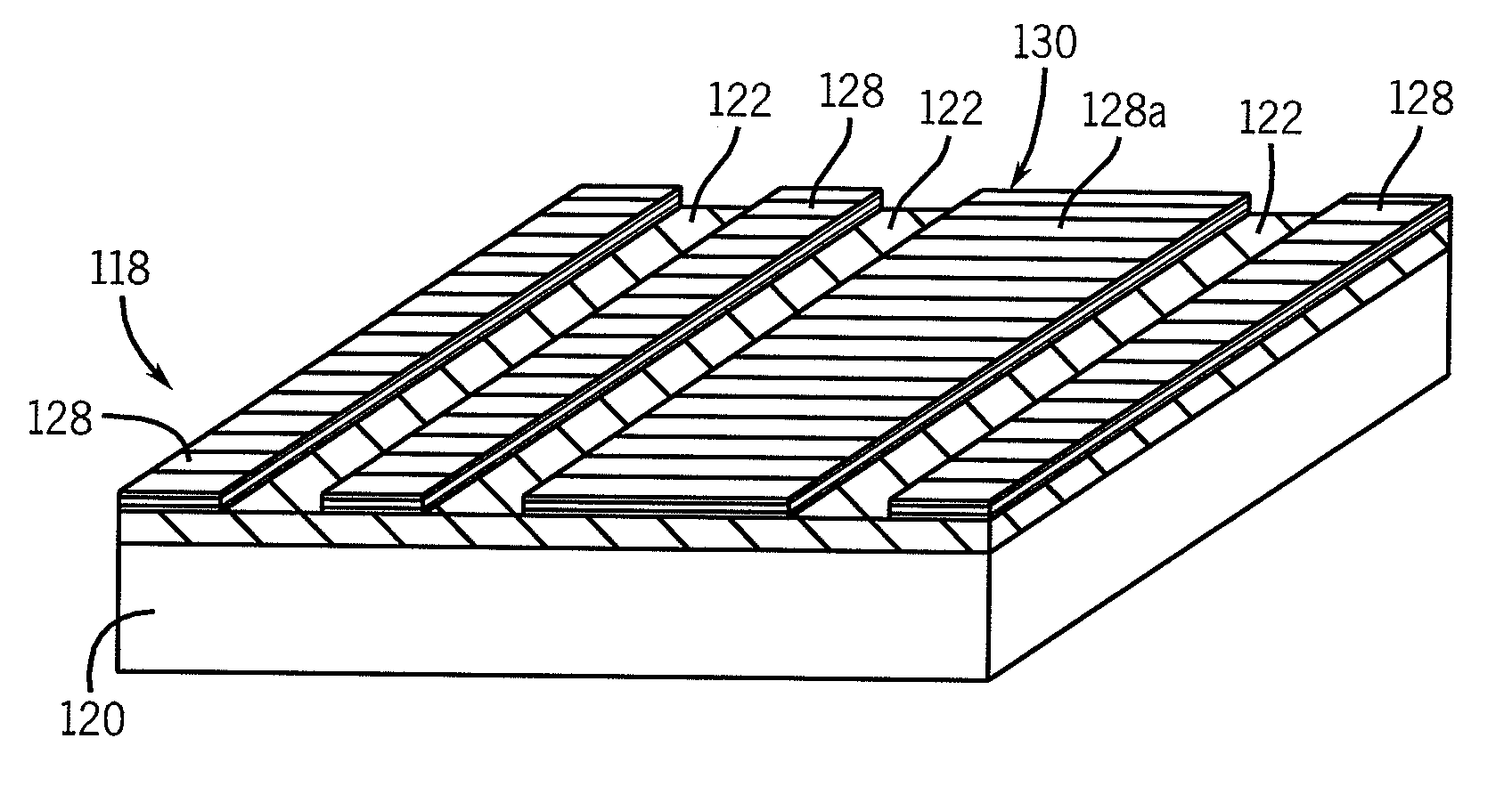
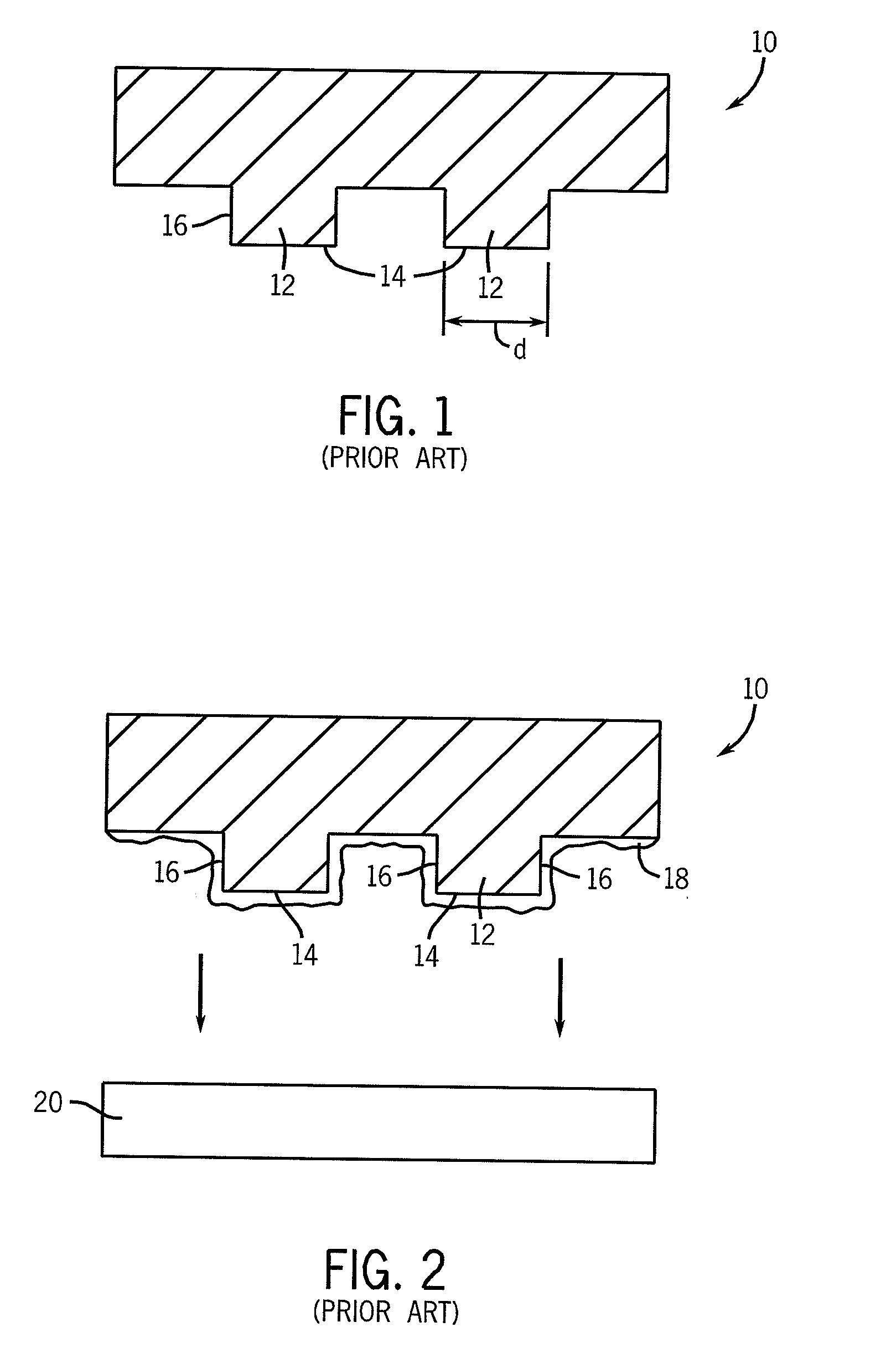
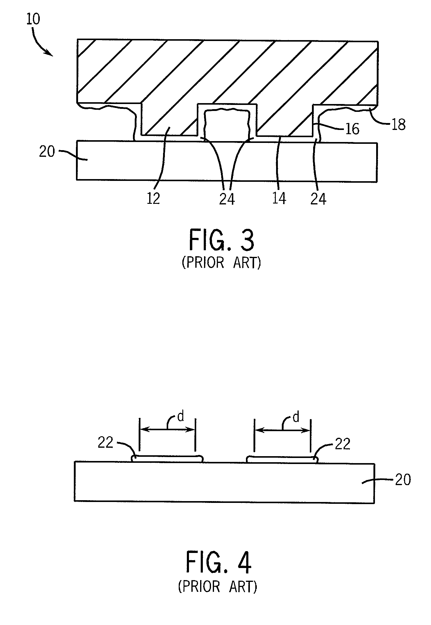
[0042]The following description with reference to the drawings provides illustrative examples of devices and methods according to embodiments of the invention. Such description is for illustrative purposes only and not for purposes of limiting the same.

[0043]In the context of the current application, the term “semiconductor substrate” or “semiconductive substrate” or “semiconductive wafer fragment” or “wafer fragment” or “wafer” will be understood to mean any construction comprising semiconductor material, including but not limited to bulk semiconductive materials such as a semiconductor wafer (either alone or in assemblies comprising other materials thereon), and semiconductive material layers (either alone or in assemblies comprising other materials). The term “substrate” refers to any supporting structure including, but not limited to, the semiconductive substrates, wafer fragments or wafers described above.

[0044]“Lo” is the inherent periodicity or pitch value (bulk period or rep...


PUM

PropertyMeasurementUnit
angleaaaaaaaaaa
feature sizeaaaaaaaaaa
depthaaaaaaaaaa

Abstract

Methods for fabricating stamps and systems for patterning a substrate, and devices resulting from those methods are provided.

Description

TECHNICAL FIELD[0001]Embodiments of the invention relate to methods, a stamp and a system for patterning a substrate by use of self-assembling block copolymers, and devices resulting from those methods.BACKGROUND OF THE INVENTION[0002]Lithography is a key process in the fabrication of semiconductor integrated circuits. Photolithography typically involves projecting an image through a reticle or mask onto a thin film of photoresist or other material that covers a semiconductor wafer or other substrate, and developing the film to remove exposed or unexposed portions of the resist to produce a pattern in subsequent processing steps. In semiconductor processing, the continual shrink in feature sizes and the increasing development of nanoscale mechanical, electrical, chemical and biological devices requires systems to produce nanoscale features. However, with conventional photolithography using light, the minimum feature size and spacing between patterns is generally on the order of the ...

Claims


Application Information

Patent Timeline
Patent Type & Authority Applications(United States)
IPC IPC(8): G03G7/00B05D5/02C08F2/46C03C25/68
CPCB05D1/283B81C99/009B81C2201/0149B82Y10/00B82Y30/00Y10T428/24802G03F7/0002G03F7/0017B41N1/08B41N3/036Y02C20/30B82Y40/00B82B3/00G03F1/68H01L21/0274
Inventor MILLWARD, DAN B.SANDHU, GURTEJ S.
Owner MICRON TECH INC
Why Eureka
Try Eureka