Method for manufacturing semiconductor device

a manufacturing method and semiconductor technology, applied in the direction of manufacturing tools, printed circuit manufacturing, soldering apparatus, etc., can solve the problems of void suppression inside the solder, difficult to clean the fluxing agent completely, and difficult to achieve both the improvement of connectivity between the solder bumps and the suppression of voids

Active Publication Date: 2010-12-23
KIOXIA CORP
View PDF4 Cites 44 Cited by
  • Summary
  • Abstract
  • Description
  • Claims
  • Application Information

AI Technical Summary

Problems solved by technology

However, in accordance with decreasing size and formation pitch of the solder bumps, it becomes difficult to clean the fluxing agent completely.
A residue of the fluxing agent results in a problem.
In this case, the oxide films are caught in interfaces between the temporarily tacked solder bumps, and it is difficult to achieve both improvement in connectivity between the solder bumps and suppression of voids to occur inside the solder bumps after being melted.

Method used


Image

  • Method for manufacturing semiconductor device
  • Method for manufacturing semiconductor device
  • Method for manufacturing semiconductor device

Examples


first embodiment

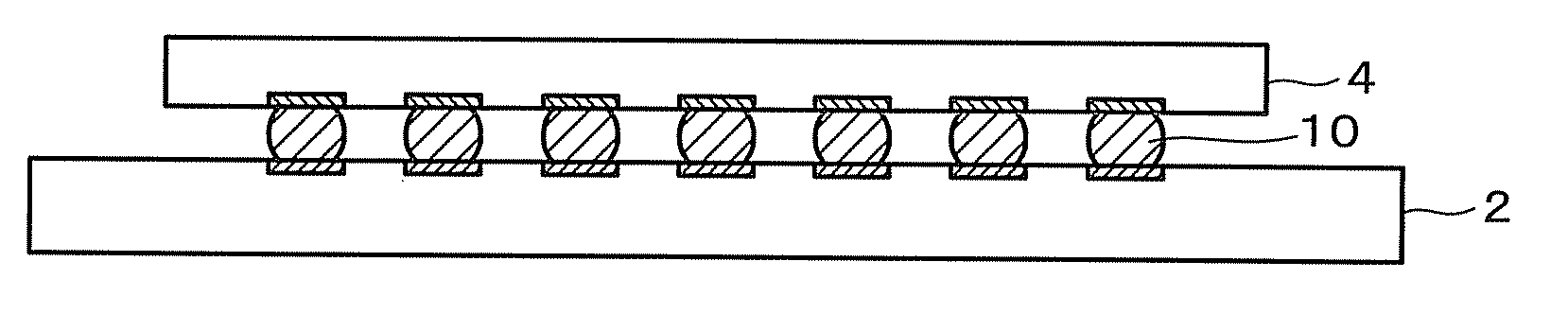
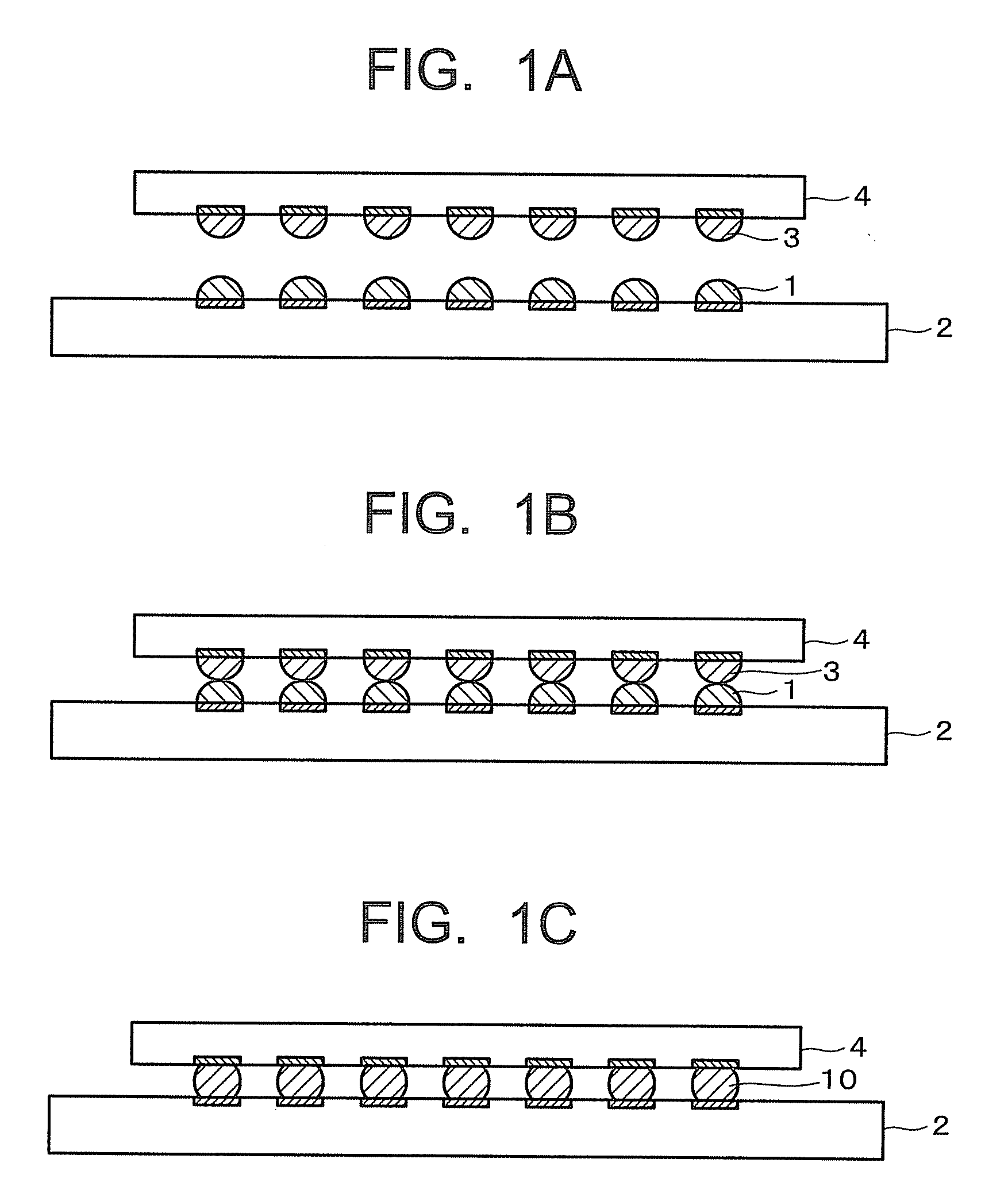
[0017]FIG. 1A to FIG. 10 are cross-sectional views showing a process of manufacturing a semiconductor device according to a first embodiment. As shown in FIG. 1A, a first substrate 2 having first solder bumps 1 and a second substrate 4 having second solder bumps 3 are prepared. The first and second substrates 2, 4 are, for example, semiconductor chips (silicon (Si) chips or the like) or silicon (Si) interposers. A combination of the first and second substrates 2, 4, which is, for example, a combination of a first semiconductor chip (2) and a second semiconductor chip (4), a combination of a Si interposer (2) and a semiconductor chip (4), a combination of a semiconductor chip (2) and a Si interposer (4), or the like, is not limited in particular.

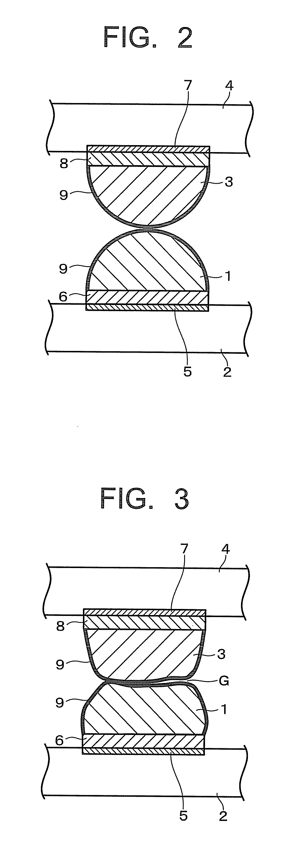
[0018]The first and second solder bumps 1, 3 are arranged in a matrix form in prescribed regions of the substrates 2, 4 respectively. The solder bumps 1, 3 as shown in FIG. 2 respectively, are formed on electrode pads 5, 7 provided on the sur...

second embodiment

[0038]In a process of manufacturing a semiconductor device in a second embodiment, similarly to the first embodiment (see FIG. 1A to FIG. 1C, FIG. 2, and FIG. 3), a second substrate 4 is stacked on a first substrate 2 while aligning first solder bumps 1 and second solder bumps 3. The first solder bumps 1 and the second solder bumps 3 are temporarily tacked. A concrete example of the substrates 2, 4, a constituent material for the solder bumps 1, 3, a method of temporarily tacking the solder bumps 1, 3, and so on are similar to those in the first embodiment.

[0039]Next, similarly to the first embodiment, a stack of the first substrate 2 and the second substrate 4, in which the solder bumps 1, 3 are temporarily tacked to each other, is disposed inside a heating furnace (reflow chamber), and then the heating furnace is evacuated to be in a reduced pressure atmosphere. Oxygen remaining inside the heating furnace oxides the solder bumps 1, 3, so that it is preferable that gas in the heati...


PUM

PropertyMeasurementUnit
pressureaaaaaaaaaa
pressureaaaaaaaaaa
temperatureaaaaaaaaaa

Abstract

In one embodiment, a first substrate having first solder bumps and a second substrate having second solder bumps are stacked while temporarily tacking the solder bumps to each other, and then a stack is disposed inside a furnace. The gas in the furnace is exhausted to be in a reduced pressure atmosphere, and then a carboxylic acid gas is introduced into the furnace. While increasing a temperature inside the furnace where the carboxylic acid gas is introduced, the gas in the furnace is exhausted to be in a reduced pressure atmosphere at a temperature in a range from a reduction temperature of oxide films by the carboxylic acid gas to lower than a melting temperature of the solder bumps. By increasing the temperature inside the furnace up to a temperature in a range of the melting temperature of the solder bumps and higher, the first solder bumps and the second solder bumps are melted and joined.

Description

CROSS REFERENCE TO RELATED APPLICATIONS[0001]This application is based upon and claims the benefit of priority from Japanese Patent Application No. 2009-146153, filed on Jun. 19, 2009; the entire contents of which are incorporated herein by reference.FIELD[0002]Embodiments described herein relate generally to a method for manufacturing a semiconductor device.BACKGROUND[0003]In recent years, in order to deal with higher pin counts, fine pitches, and increase in signal speed of semiconductor chips, there are used semiconductor devices employing flip-chip connection as a mounting method having short wiring and connection lengths. When the flip-chip connection is applied to connection between semiconductor chips and connection between a semiconductor chip and a silicon interposer, solder bumps are formed on electrode pads of upper and lower chips (semiconductor chips or silicon interposers) respectively, the chips are aligned to face these solder bumps and stacked, and then the solder b...

Claims


Application Information

Patent Timeline
Patent Type & Authority Applications(United States)
IPC IPC(8): B23K31/02
CPCB23K1/0016Y10T29/49149H01L24/13H01L24/81H01L2224/13099H01L2224/16H01L2224/81065H01L2224/81193H01L2224/81801H01L2224/81986H01L2924/01029H01L2924/01078H01L2924/01082H01L2924/01005H01L2924/01006H01L2924/01033H01L2924/01047H01L2924/0105H01L2924/014H01L2924/10253B23K1/008Y10T29/49144H01L2224/13111H01L2224/13109H01L2224/131H01L2924/00H01L2924/00014H01L2924/01083H01L24/05H01L2224/05001H01L2224/05026H01L2224/05568H01L2224/056H01L2224/05099
Inventor SAWADA, KANAKOAOKI, HIDEOKOMUTA, NAOYUKIOGISO, KOJI
Owner KIOXIA CORP
Why Eureka
Try Eureka