
Eureka
For R&D, Eureka makes reading and utilizing patents & technical documents easy.
Eureka AIR
Designed for self-driven R&D workflows. Generate viable solutions, solve complex R&D challenges, empower your innovation with AI.

Eureka Materials
Designed for material experts only. Revolutionize your material R&D, from search, analyze, to developing new materials.

TechResearch
Generate reliable direction feasibility study reports for your R&D in just a few steps.

TechSeek
Discover and master advanced knowledge NOW. Basics, ideas, possibilities, all at once.

TechMind
As an expert in R&D Theories, TechMind can generates customized viable solutions instantly.

TechRisk
Analyze your overall solution with one click, know your potential R&D risks in advance.

TechMonitor
Get weekly tech updates, stay abreast of the latest tech innovations and key insights.
Semiconductor device assembly having a stress-relieving buffer layer
- Summary
- Abstract
- Description
- Claims
- Application Information
AI Technical Summary
Benefits of technology
Problems solved by technology
Method used
Image

Examples
Embodiment Construction
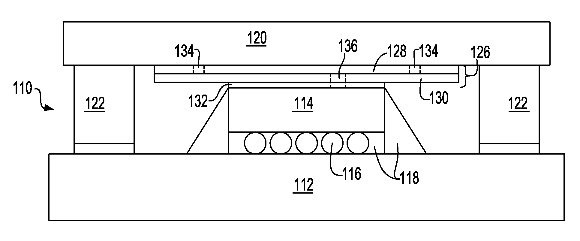
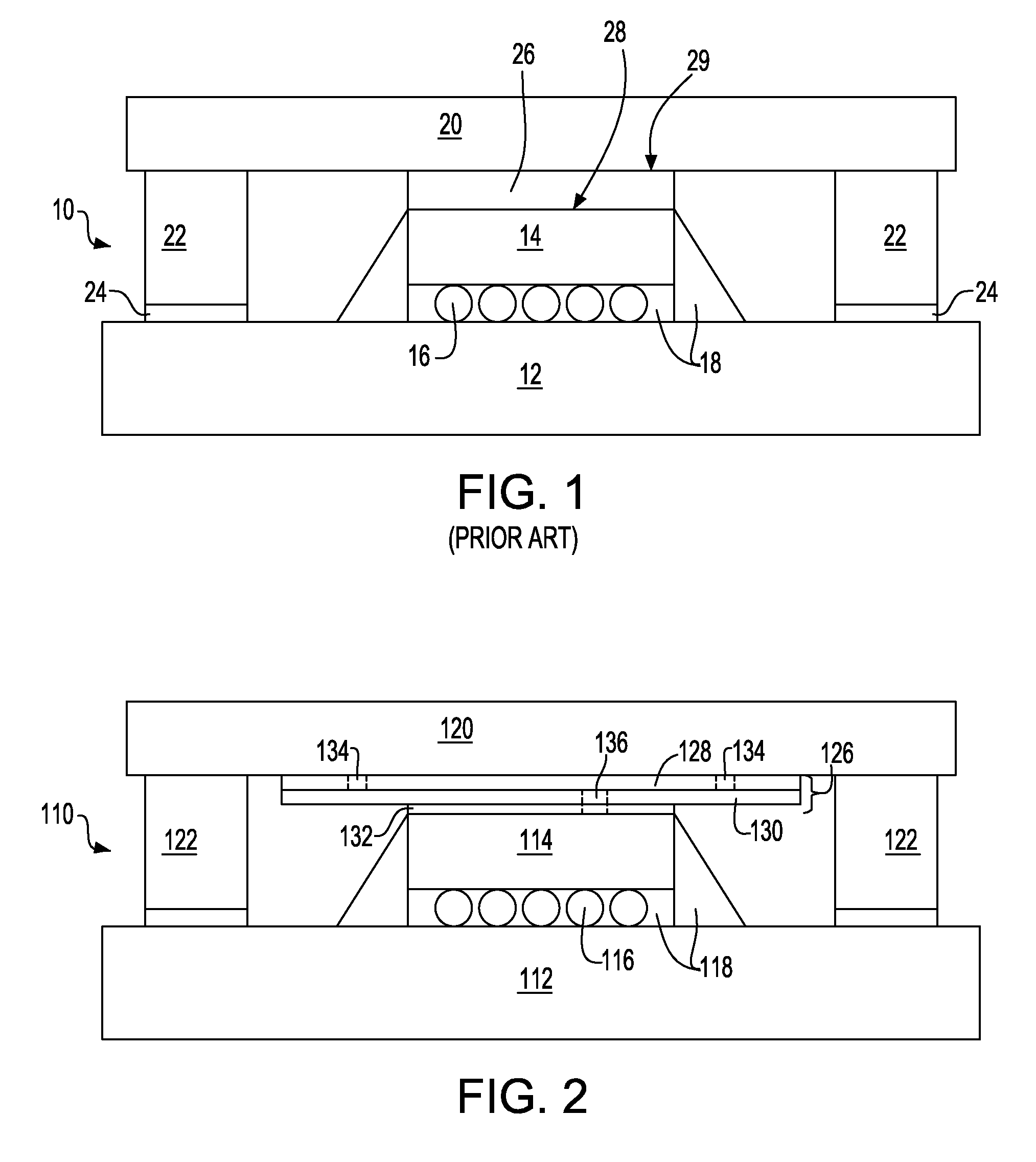
[0021]Referring to the Figures in more detail, and particularly referring to FIG. 1, there is shown a side view of a prior art semiconductor device assembly 10. The semiconductor device assembly 10 includes a chip carrier substrate 12, such as an organic chip carrier, upon which a chip 14, hereafter referred to as a semiconductor device, is mounted in the so-called flip chip position. By flip chip, it is meant that the semiconductor device 14 is mounted active side down and the semiconductor device 14 makes connections to the substrate 12 through solder balls 16 or other well-known electrical connections. There may also be a conventional underfill material 18. The semiconductor device assembly 10 may also include a lid or heat spreader 20 (hereafter collectively referred to as just “heat spreader”) which removes heat generated by the semiconductor device 14. The heat spreader 20 may be supported by legs 22 which are firmly attached to the substrate 12 by adhesive 24. Lastly, in orde...
PUM
 Abstract
Description
Claims
Application Information
 - R&D Engineer
- R&D Manager
- IP Professional
- Industry Leading Data Capabilities
- Powerful AI technology
- Patent DNA Extraction
Browse by: Latest US Patents, China's latest patents, Technical Efficacy Thesaurus, Application Domain, Technology Topic, Popular Technical Reports.
© 2024 PatSnap. All rights reserved.Legal|Privacy policy|Modern Slavery Act Transparency Statement|Sitemap|About US| Contact US: help@patsnap.com