Power saving termination circuits for dram modules

a termination circuit and dram module technology, applied in the direction of power consumption reduction, pulse technique, instruments, etc., can solve the problems of significant power consumption of termination resistors and additional power consumption, and achieve the effect of reducing the power consumed by termination circuits, less power, and reducing reflection effects

Inactive Publication Date: 2010-12-30
UNIRAM TECH
View PDF18 Cites 35 Cited by
  • Summary
  • Abstract
  • Description
  • Claims
  • Application Information

AI Technical Summary

Benefits of technology

[0012]The primary objective of this invention is, therefore, to reduce the power consumed by termination circuits for DRAM modules. Another objective is to provide power saving termination circuits for PCIe, SATA, or MIPI interfaces. These and other objectives are achieved by using capacitor(s) connected in series with resistor(s) as termination circuits. The resulting termination circuits are capable of reducing reflection effects while consuming much less power than prior art termination resistors.

Problems solved by technology

Termination resistors are effective in reducing distortions caused by reflection, but they consume additional power.
We can see the trend that more and more termination resistors are used for newer generations of DRAM modules; these termination resistors start to consume significant power.

Method used


Image

  • Power saving termination circuits for dram modules
  • Power saving termination circuits for dram modules
  • Power saving termination circuits for dram modules

Examples


Embodiment Construction

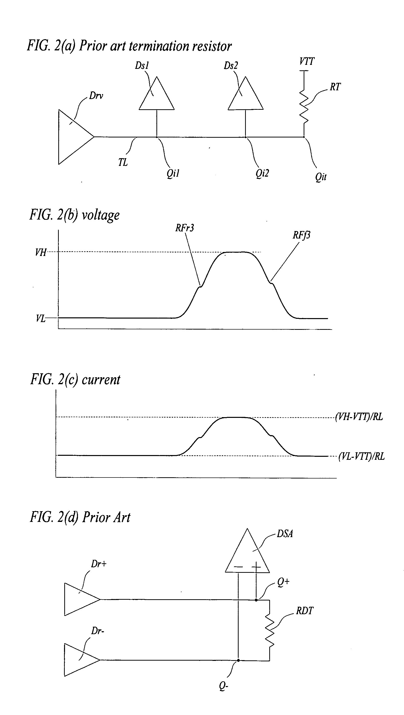
[0027]FIGS. 5(a-d) are simplified symbolic diagrams illustrating the operation principles of RC termination circuits. FIG. 5(a) shows a driver (Drv) driving an electrical wire (TL) that is connected to two sensors (Ds1, Ds2) at two different points (Qi1, Qi2). The end point (Qit) of the electrical wire (TL) is connected to a resistor (RTc) that is connected in series with a capacitor (CT) while connecting to a voltage source (VTT). The voltage of this voltage source (VTT) can be the same as the termination voltage of prior art termination resistors; it also can be a different voltage. We will call these types of termination circuits that comprise at least one capacitor and one resistor connected in series as “RC termination circuits”. The RC termination circuits are less sensitive to the voltage values of voltage sources than prior art termination resistors. This circuit shown in FIG. 5(a) is nearly identical to the circuit in FIG. 2(a) except that the termination resistor (RT) in F...


PUM


Abstract

The present invention provides power saving methods by replacing termination resistors used to support SSTL DRAM interfaces with RC termination circuits; the RC termination circuits consumes significant less power relative to prior art termination resistors at low frequency and behave as a matching impedance at high frequency. Similar methods and structures are also applicable for PCIe, SATA, or MIPI differential interfaces.

Description

BACKGROUND OF THE INVENTION[0001]The present invention relates generally to termination circuits used to reduce the effects of reflection at the ends of electrical wires, and more particularly to termination circuits used for “dynamic random access memory” (DRAM) interface signals.[0002]The signal transfer rates for DRAM “stub series terminated logic” (SSTL) interfaces have been progressing exponentially. Initial generation “double data rate” (DDR) DRAM supports data transfer rates at or lower than 400 “million bits per second” (Mpbs) per signal line with clock frequencies at or lower than 200 “million cycles per second” (MHZ). The second generation DDR2 DRAM supports data transfer rate up to 800 Mbps with clock frequencies up to 400 MHZ. Current art third generation DDR3 DRAM supports 1.6 billion bits per second (Gbps) with clock frequencies up to 800 MHZ. The present invention will focus on DRAM modules with clock frequencies higher than 300 MHZ. Operating at such high frequencies...

Claims


Application Information

Patent Timeline
Patent Type & Authority Applications(United States)
IPC IPC(8): H03K17/16H01L21/20
CPCG11C7/1048G11C7/1066G11C11/4093H03K19/0013H01L28/20H01L28/40H03K19/0005H01L27/10897H10B12/50
Inventor SHAU, JENG-JYE
Owner UNIRAM TECH
Why Eureka
Try Eureka