Front to back resistive random access memory cells

a random access and memory cell technology, applied in the field of front to back resistive random access memory cells, can solve the problems of large overhead circuitry, limiting the ways in which nvm storage can be applied in user designs, and requiring flash technology to require a large amount of overhead circuitry

Active Publication Date: 2011-01-06
MICROSEMI SOC
View PDF99 Cites 129 Cited by
  • Summary
  • Abstract
  • Description
  • Claims
  • Application Information

AI Technical Summary

Problems solved by technology

Unfortunately, flash technology requires a large amount of overhead circuitry, such as complex row and column drivers, programming control logic, and charge pumps to generate the high voltages required for programming and erase operations.
This limits the ways the NVM storage can be applied in user designs, e.g. by limiting the bandwidth or number of ports of the NVM storage.
If the tristate driver used for programming a track is turned on it might fight with the logic or routing buffer output that normally drives the same track.
Of course, some means could be provided to override or disconnect the normal output, but this generally costs area and delay.
This limits the performance and routability of the architecture.
As a result significant voltages may occur across a programmed switch, which may cause its resistance to increase (read disturb of on-switches).
This is inefficient for layout, since the common terminal of the two devices comprising the switch will need to be connected to an addressing transistor through a contact on the lowest layer of metal.

Method used


Image

  • Front to back resistive random access memory cells
  • Front to back resistive random access memory cells
  • Front to back resistive random access memory cells

Examples


Embodiment Construction

[0064]Persons of ordinary skill in the art will realize that the following description of the present invention is illustrative only and not in any way limiting. Other embodiments of the invention will readily suggest themselves to such skilled persons.

[0065]According to an aspect of the present invention, area-efficient solid electrolyte RRAM device structures are disclosed. The RRAM devices according to the present invention are more manufacturable and are more reliable than prior-art RRAM devices.

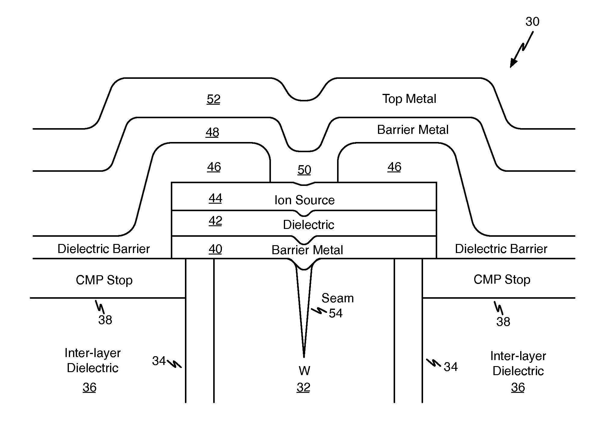
[0066]Referring now to FIG. 6, a cross-sectional diagram shows the structure of an illustrative RRAM device 30 according to the present invention presenting one way to reduce the seam problem illustrated in FIG. 5. The RRAM device 30 illustrated in FIG. 6 can be incorporated into a process using tungsten-filled vias.

[0067]RRAM device 30 is formed over a tungsten via 32. Tungsten via 32 is surrounded by a barrier layer 34 and is formed in inter-metal dielectric layer 36. A CMP stop layer ...


PUM


Abstract

A resistive random access memory device formed on a semiconductor substrate comprises an interlayer dielectric having a via formed therethrough. A chemical-mechanical-polishing stop layer is formed over the interlayer dielectric. A barrier metal liner lines walls of the via. A conductive plug is formed in the via. A first barrier metal layer is formed over the chemical-mechanical-polishing stop layer and in electrical contact with the conductive plug. A dielectric layer is formed over the first barrier metal layer. An ion source layer is formed over the dielectric layer. A dielectric barrier layer is formed over the ion source layer, and includes a via formed therethrough communicating with the ion source layer. A second barrier metal layer is formed over the dielectric barrier layer and in electrical contact with the ion source layer. A metal interconnect layer is formed over the barrier metal layer.

Description

CLAIM FOR PRIORITY[0001]This application claims the benefit of U.S. Provisional Application Ser. No. 61 / 222,708, filed on Jul. 2, 2009, the entirety of which is incorporated by reference herein.BACKGROUND[0002]The majority of commercial programmable logic devices such as FPGAs use one-bit SRAM cells to store their configuration data. However SRAM cells consume significant static power, and lose their state when powered off. In addition, because SRAM cells need to be loaded at power-up, the configuration data is difficult to keep secure.[0003]Using a non-volatile memory device to store the configuration data for programmable logic devices avoids these two problems. Many types of non-volatile memory devices are known. See for example Burr, et al., IBM J. Res. & Dev. Vol. 52 No. 4 / 5, 2008, “A Novel Resistance Memory with High Scalability and Nanosecond Switching”, IEDM 2007. Various non-volatile memory devices are known, and some of them are more suitable than others for use as configu...

Claims


Application Information

Patent Timeline
Patent Type & Authority Applications(United States)
IPC IPC(8): H01L45/00
CPCH01L27/2436H01L27/2463H01L45/085H01L45/1266H01L45/141H01L45/142H01L45/1253H01L45/1616H01L45/1625H01L45/1675H01L45/122H01L45/1233Y10S438/90H01L45/149H03K19/17724H03K19/1776G11C13/0011H10B63/30H10B63/80H10N70/245H10N70/826H10N70/8416H10N70/882H10N70/8822H10N70/8845H10N70/023H10N70/026H10N70/063H10N70/011H10N70/821H10N70/841H10N70/24
Inventor GREENE, JONATHANHAWLEY, FRANK W.MCCOLLUM, JOHN
Owner MICROSEMI SOC
Why Eureka
Try Eureka