
Binary Logic Utilizing MEMS Devices

Active Publication Date: 2011-01-06
QORVO US INC
View PDF11 Cites 18 Cited by
  • Summary
  • Abstract
  • Description
  • Claims
  • Application Information

AI Technical Summary

Benefits of technology

[0018]Embodiments disclosed herein generally relate to switches that utilize micro-electromechanical systems (MEMS). By replacing transistors in many devices with switches such as MEMS switches, the devices may be used for logic applications. MEMS switches may be used in devices such as FPGAs, NAND devices, nvSRAM devices, AM

Problems solved by technology

To date, MEMS-only design has not been achieved for NVM devices.
These technologies all have limitations with respect to speed and / or endurance.
However, relying on a battery is not a real fail-safe option and regular replacements of batteries is required and expensive.
However, the memory cells are very large (i.e., about twice the size of a normal SRAM cell), while also the EEPROM process steps add additional costs, resulting in a memory with a cost price of about 3 times the cost of standard SRAM memory.
Because of the NMOS device in each memory cell, area underneath the MEMS could not be utilized.
Third, an ‘electrical fuse’, which is a special wire on the chip, which can be electrically blown-up to become a high impedance.
Fourth, blowing-up a transistor, which becomes a high impedance value versus a low impedance, when normally switched on.
One of the issues with one-time programmable devices is that they can't be tested in both states prior to releasing it to a customer.

Method used


Image

  • Binary Logic Utilizing MEMS Devices
  • Binary Logic Utilizing MEMS Devices
  • Binary Logic Utilizing MEMS Devices

Examples


Embodiment Construction

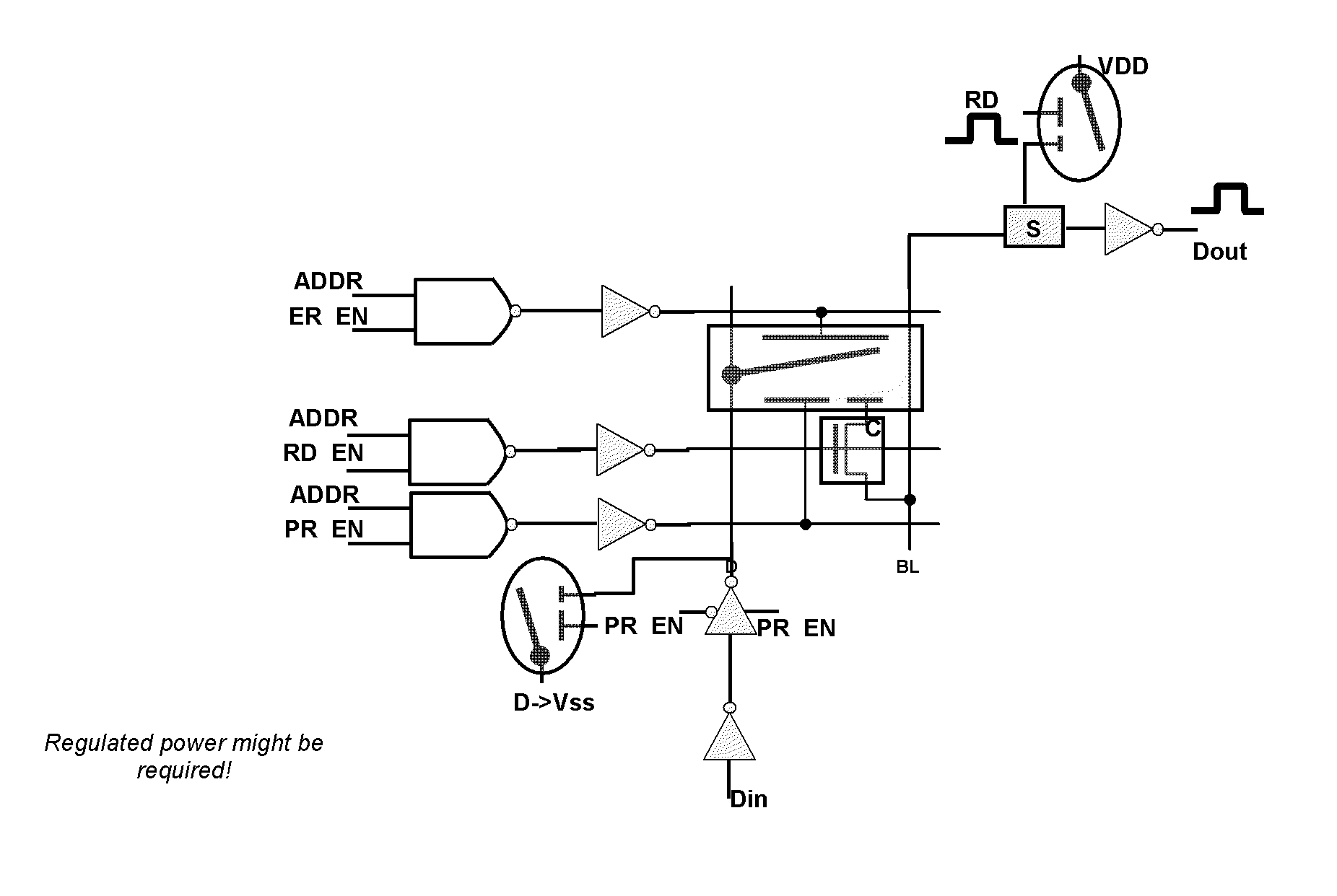
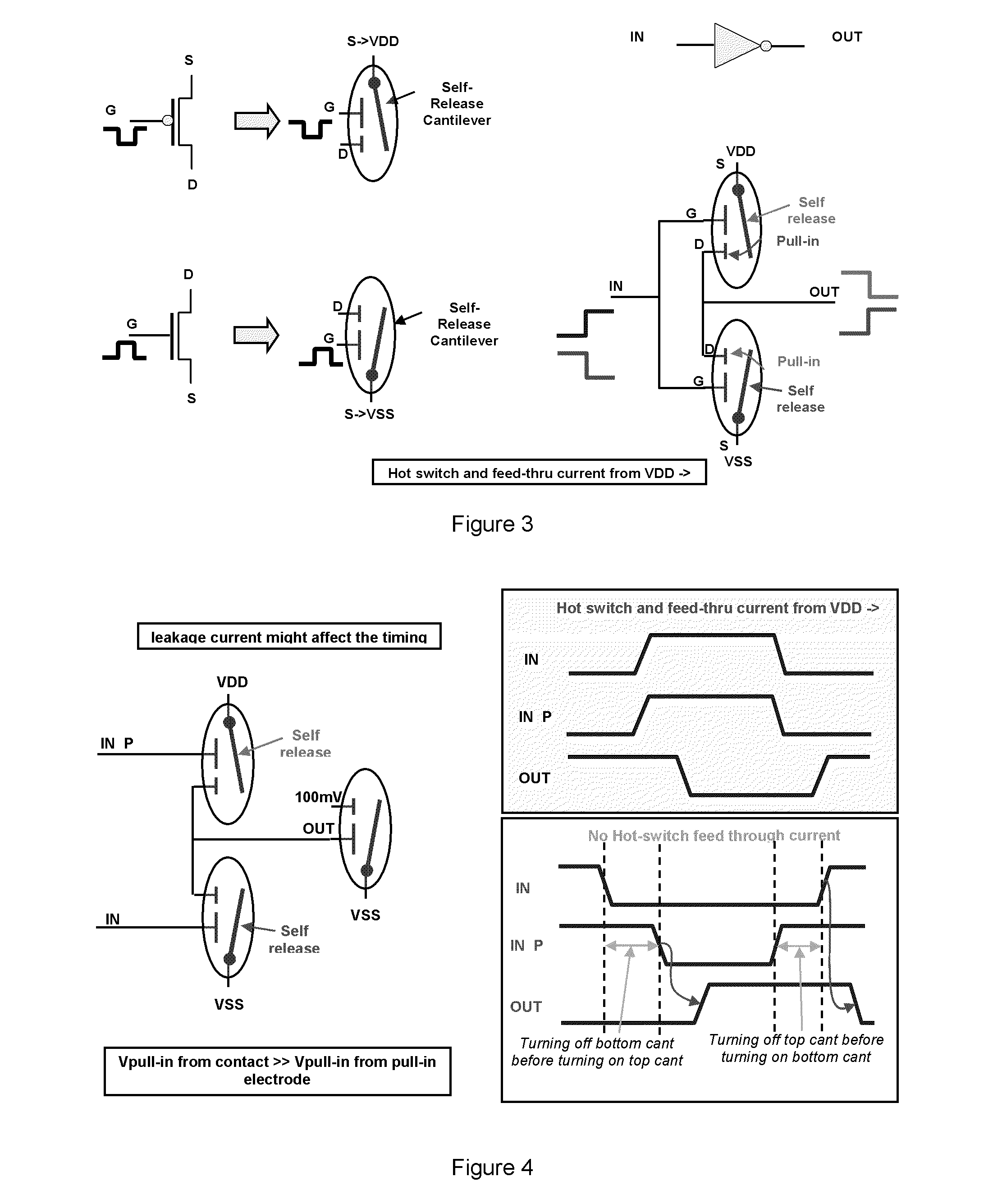
[0080]Embodiments disclosed herein generally relate to switches that utilize micro-electromechanical systems (MEMS). By replacing transistors in many devices with switches such as MEMS switches, the devices may be used for logic applications. MEMS switches may be used in devices such as FPGAs, NAND devices, nvSRAM devices, AMS chips and general memory logic devices. The benefit of utilizing MEMS devices in place of transistors is that the transistors utilize more space on the chip. Additionally, the MEMS devices can be formed in the BEOL without having any negative impacts on the FEOL or necessitating the use of additional layers within the chip.

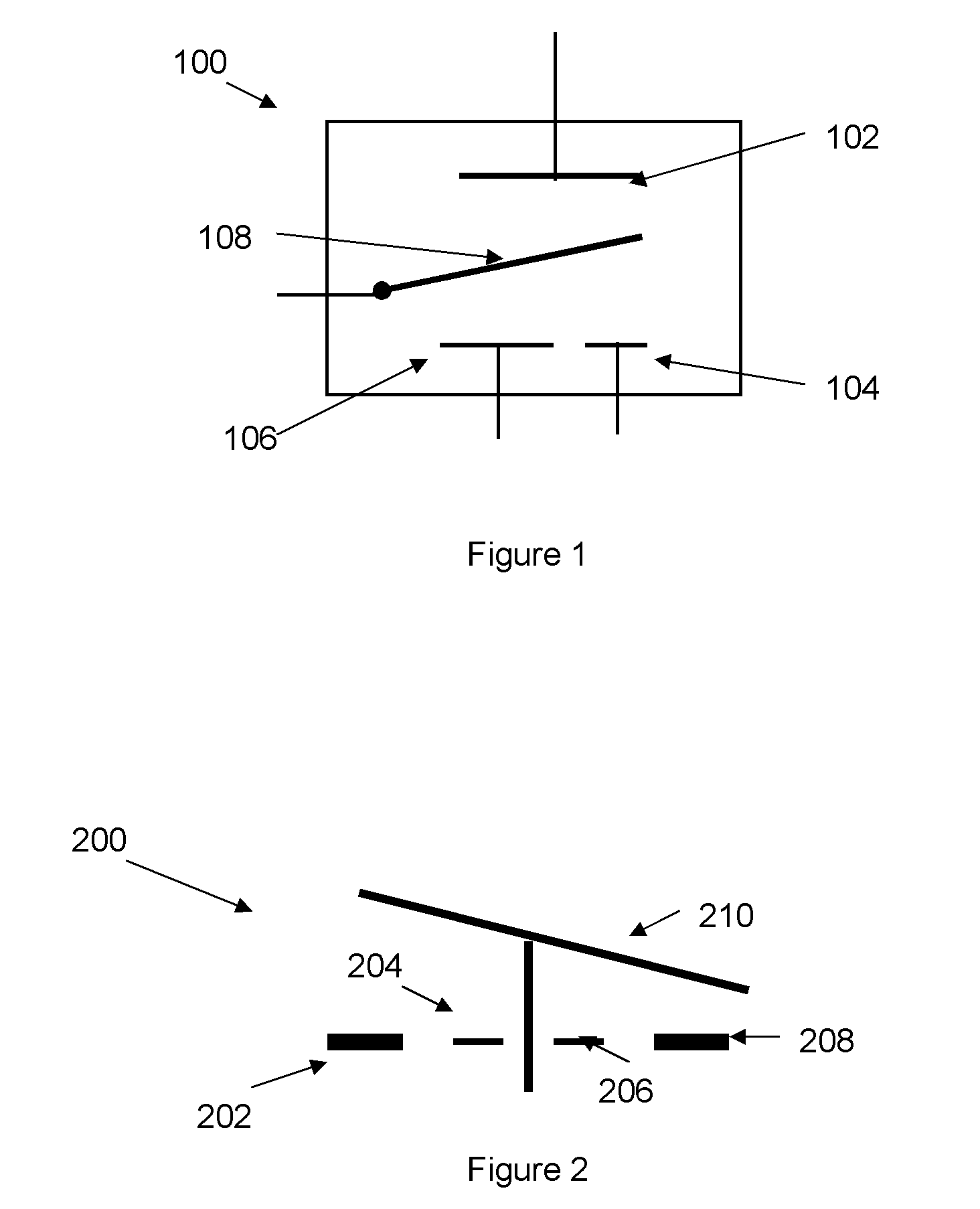
[0081]Throughout the description herein, reference will be made to a cantilever-type MEMS device and a rocker-type MEMS device. FIG. 1 shows a cantilever-type MEMS device 100. The cantilever-type MEMS device 100 includes a pull-up electrode 102, a contact electrode 104, a pull-in electrode 106 and a cantilever electrode 108. During operation...


PUM


Abstract

Embodiments disclosed herein generally relate to switches that utilize micro-electromechanical systems (MEMS). By replacing transistors in many devices with switches such as MEMS switches, the devices may be used for logic applications. MEMS switches may be used in devices such as FPGAs, NAND devices, nvSRAM devices, AMS chips and general memory logic devices. The benefit of utilizing MEMS devices in place of transistors is that the transistors utilize more space on the chip. Additionally, the MEMS devices can be formed in the BEOL without having any negative impacts on the FEOL or necessitating the use of additional layers within the chip.

Description

CROSS-REFERENCE TO RELATED APPLICATIONS[0001]This application claims benefit of U.S. Provisional Patent Application Ser. No. 61 / 222,476 (1912.040013), filed Jul. 1, 2009, which is herein incorporated by reference.BACKGROUND OF THE INVENTION[0002]1. Field of the Invention[0003]Embodiments disclosed herein generally relate to switches that utilize micro-electromechanical systems (MEMS).[0004]2. Description of the Related Art[0005]Currently, MEMS-based non-volatile memory (NVM) design requires all peripheral circuits and the pass gate in each memory cell to be a complementary metal oxide semiconductor (CMOS) device. To further utilize the advantage of MEMS-based design between interconnect layers, one needs to be able to do all of the simple logics with MEMS-only design. At the very end, there will be the interface design between MEMS design and CMOS design. To date, MEMS-only design has not been achieved for NVM devices.[0006]One example of a NVM device is a non-volatile static random...

Claims


Application Information

Patent Timeline
IPC IPC(8): G11C14/00H03K19/094G11C16/04
CPCG11C14/0054H03K19/02G11C23/00
Inventor SCHEPENS, CORNELIUS PETRUS ELISABETHKHIEU, CONG QUOCVAN KAMPEN, ROBERTUS PETRUS
Owner QORVO US INC
Learn More