
Method of manufacturing semiconductor device and pattern formation method

Inactive Publication Date: 2011-01-06
SONY CORP
View PDF4 Cites 10 Cited by
  • Summary
  • Abstract
  • Description
  • Claims
  • Application Information

AI Technical Summary

Benefits of technology

[0017]Therefore, it may be difficult to manufacture a semiconductor device with high efficiency or realize cost reduction.
[0018]Accordingly, it is desirable to provide a method of manufacturing a semiconductor device and a pattern formation method by which manufacturing efficiency can be improved, and cost reduction can be readily realized.
[0024]According to the embodiments of the present invention, it is possible to provide a method of manufacturing a semiconductor device and a pattern formation method capable of improving manufacturing efficiency and readily realizing cost reduction.

Problems solved by technology

However, in the aforementioned insolubilization, since dedicated materials or equipment are demanded, cost may disadvantageously increase.
However, in these methods, the shape of the resist pattern may be deformed by heat shearing.
Since it is difficult to process the entire surface of a wafer with a constant condition, or a plurality of resist patterns are laminated, it may be difficult to obtain a demanded insolubilization capability.
Specifically, in the UV-curing, since broadband light is irradiated from the Hg lamp light source, it is difficult to obtain sufficient insolubility of the resist pattern against a resist solvent or a developer.
In addition, some disadvantages such as generation of a discharge gas or necessity of dedicated equipment are generated.
Therefore, it may be difficult to manufacture a semiconductor device with high efficiency or realize cost reduction.

Method used


Image

  • Method of manufacturing semiconductor device and pattern formation method
  • Method of manufacturing semiconductor device and pattern formation method
  • Method of manufacturing semiconductor device and pattern formation method

Examples


first embodiment

1. First Embodiment

(A) Manufacturing Method

[0055]Main components of a method of manufacturing a semiconductor device will be described.

[0056]FIGS. 1 and 2A to 9B illustrate a method of manufacturing a semiconductor device according to the first embodiment of the present invention.

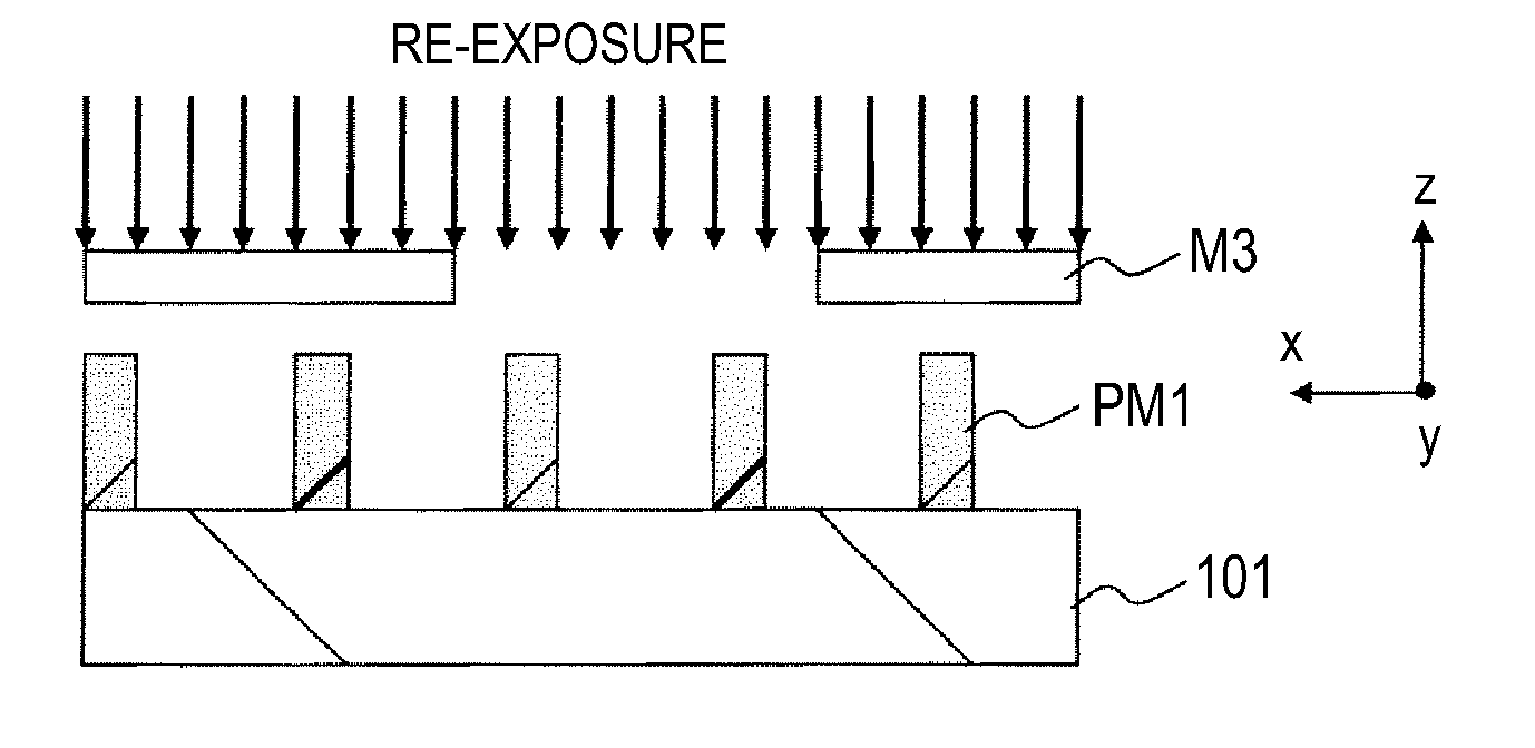
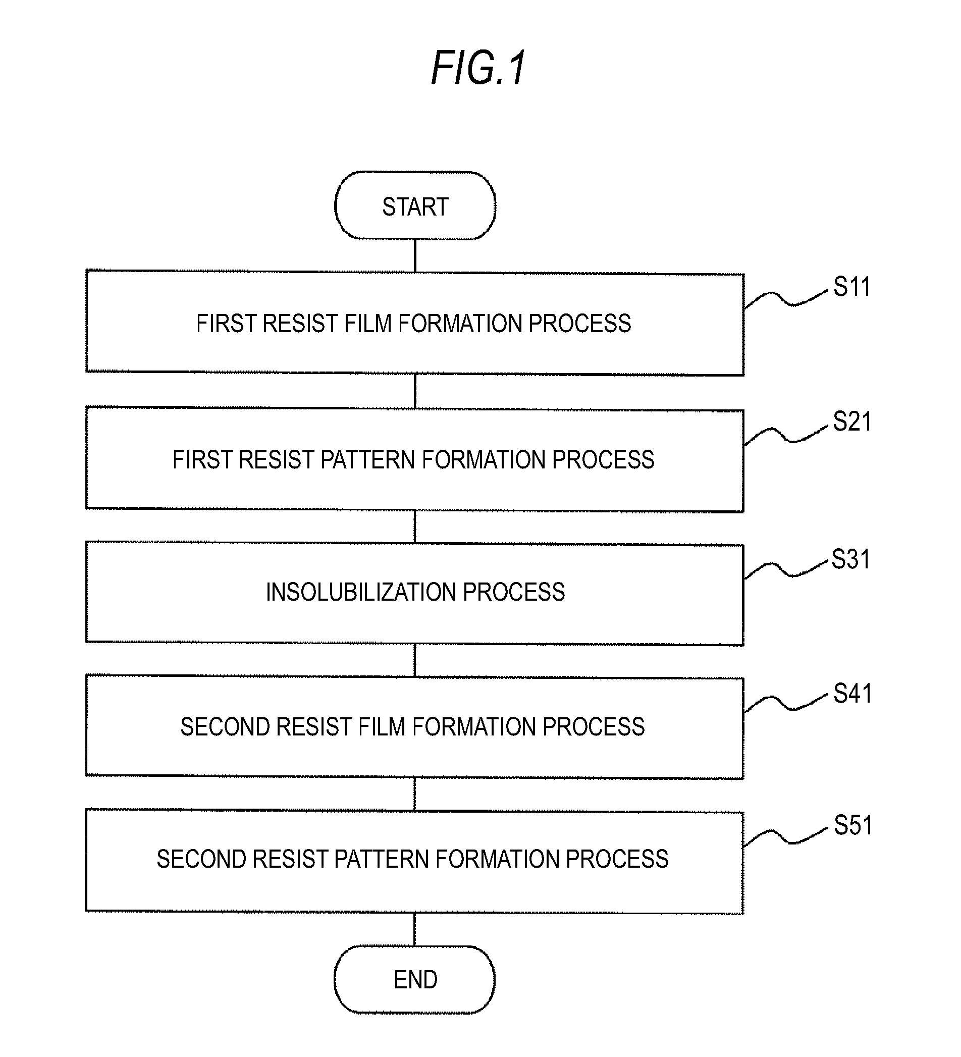
[0057]Here, FIG. 1 is a flowchart illustrating a method of manufacturing a semiconductor device according to the present embodiment.

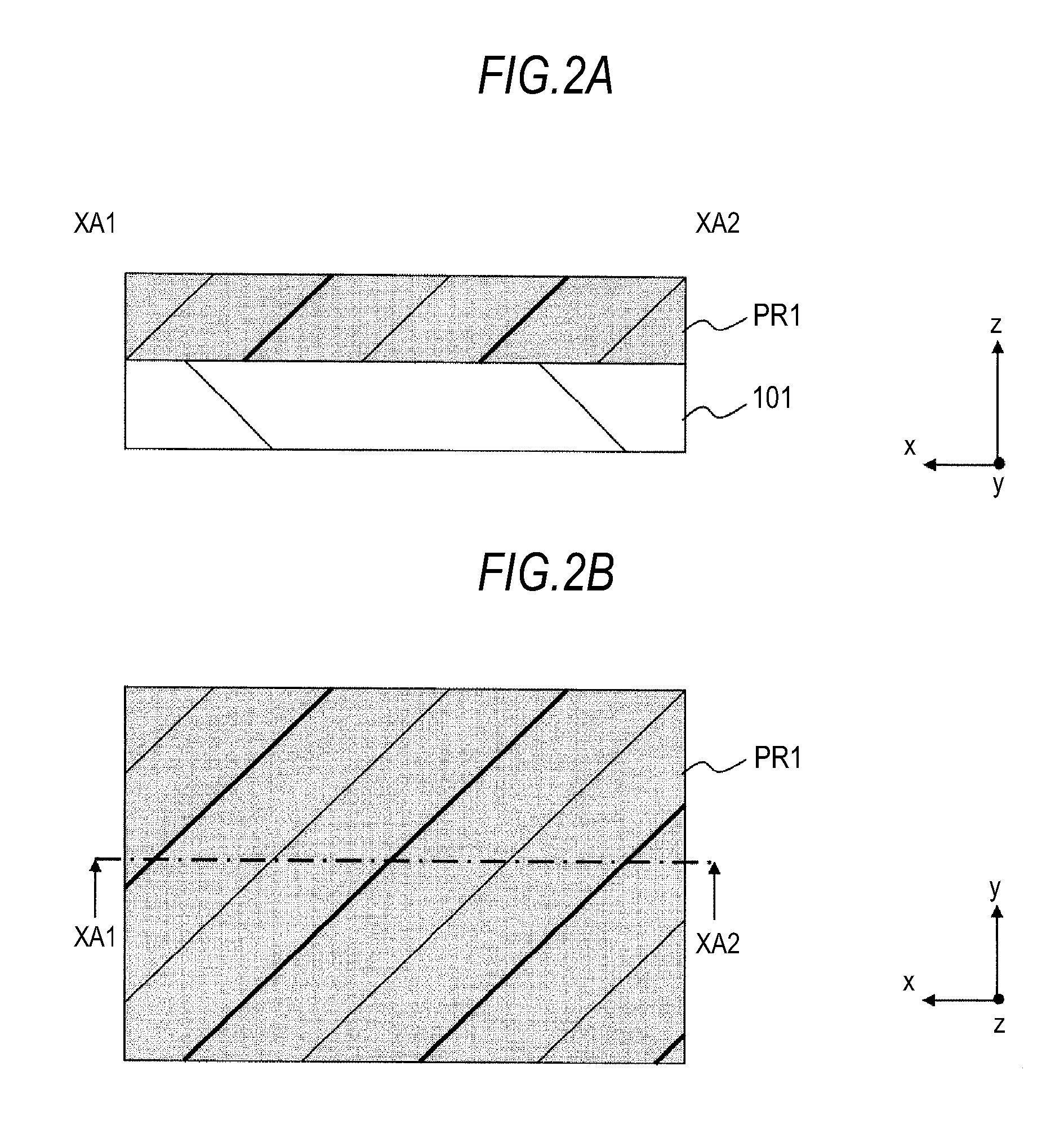
[0058]FIGS. 2A to 9B illustrate each process of manufacturing a semiconductor device according to the first embodiment of the invention. FIGS. 2A, 3A, 4A, 5A, 6A, 7A, 8A, and 9A are cross-sectional views, and FIGS. 2B, 3B, 4B, 5B, 6B, 7B, 8B, and 9B are top plan views. FIGS. 2A, 3A, 4A, 5A, 6A, 7A, 8A, and 9A illustrate cross-sections along the lines XA1-XA2 of FIGS. 2B, 3B, 4B, 5B, 6B, 7B, 8B, and 9B, respectively.

(A-1) First Resist Film Formation Process (S11)

[0059]First, as shown in FIG. 1, a first resist film formation process is performed (S11).

[0060]Here, as shown in FIGS...

modification 1

(C-1) Modification 1

[0146]FIGS. 12A and 12B illustrate a modification of the first embodiment of the present invention.

[0147]FIG. 12A is a cross-sectional view, and FIG. 12B is a top plan view. FIG. 12A illustrates a cross-section along the line XB1-XB2 of FIG. 12B.

[0148]As shown in FIGS. 12A and 12B, the first resist pattern PM1 is formed as described above. In addition, insolubilization is performed for the first resist pattern PM1 as described above.

[0149]As shown in FIGS. 12A and 12B, in the second resist pattern PM2b, unlike the aforementioned case, a plurality of patterns extending in a lateral direction (x) are lined in a longitudinal direction (y) with the same interval. Here, the second resist pattern PM2 is formed such that at least a part of the second resist pattern PM2b is laminated in the first resist pattern PM1.

[0150]As such, a hole pattern may be formed by overlappingly forming a line-and-space pattern having two layers perpendicular to each other. As a result, it i...

modification 2

(C-2) Modification 2

[0151]FIGS. 13A and 13B illustrate a modification of the first embodiment of the present invention.

[0152]FIG. 13A is a cross-sectional view, and FIG. 13B is a top plan view. FIG. 13A illustrates a cross-section along the line XC1-XC2 of FIG. 13B.

[0153]As shown in FIGS. 13A and 13B, the first resist pattern PM1 is formed as described above. Similar to the aforementioned case, insolubilization is performed for the first resist pattern PM1.

[0154]Then, as shown in FIGS. 13A and 13B, for the second resist pattern PM2c, unlike the aforementioned case, a pattern having a square plane is formed to have a matrix shape lined in a longitudinal direction (y) and a lateral direction (x).

[0155]As such, a complicated pattern difficult to be formed at a single time may be formed by dividing the process into two stages. In other words, this modification is effectively applicable to a case where densely pitched patterns and sparsely pitched patterns are mixedly provided, and a pro...


PUM


Abstract

A method of manufacturing a semiconductor device, includes: a first resist film formation process of forming a first resist film on a processing target surface using a positive-type photoresist material; a first resist pattern formation process of forming a first resist pattern by performing development after exposure in which light is irradiated onto the first resist film; a second resist film formation process of forming a second resist film on the processing target surface, where the first resist pattern is formed, using a photoresist material; and a second resist pattern formation process of forming a second resist pattern by performing exposure in which light is irradiated onto the second resist film and then performing development. The method further includes an insolubilization process for insolubilizing the first resist pattern against a developer and a solvent of a photoresist material used in the second resist pattern formation process.

Description

BACKGROUND OF THE INVENTION[0001]1. Field of the Invention[0002]The present invention relates to a method of manufacturing a semiconductor device and a method of forming a pattern. Particularly, the present invention relates to a method of manufacturing a semiconductor device and a method of forming a pattern using a double-patterning method.[0003]2. Description of the Related Art[0004]In order to manufacture the semiconductor device, a fine fabrication process is performed by forming fine patterns or the like using a lithography technology.[0005]In the aforementioned process, first, a resist film made of a photosensitive material is formed on the surface as a target of the micro-fabrication process. Then, a pattern image is transferred to the resist film by performing exposure. Subsequently, development is performed for the resist film where the pattern image is transferred to form a resist pattern from the resist film. In addition, a micro-patterning is performed, for example, by ...

Claims


Application Information

Patent Timeline
IPC IPC(8): G03F7/20
CPCG03F7/40G03F7/0035
Inventor MIYAMOTO, HIROYUKI
Owner SONY CORP
Features
  • Generate Ideas
  • Intellectual Property
  • Life Sciences
  • Materials
  • Tech Scout
  • Unparalleled Data Quality
  • Higher Quality Content
  • 60% Fewer Hallucinations
Learn More