

Semiconductor device and the method for manufacturing the same
- Summary
- Abstract
- Description
- Claims
- Application Information
AI Technical Summary
Benefits of technology
Problems solved by technology
Method used
Image

Examples
first embodiment
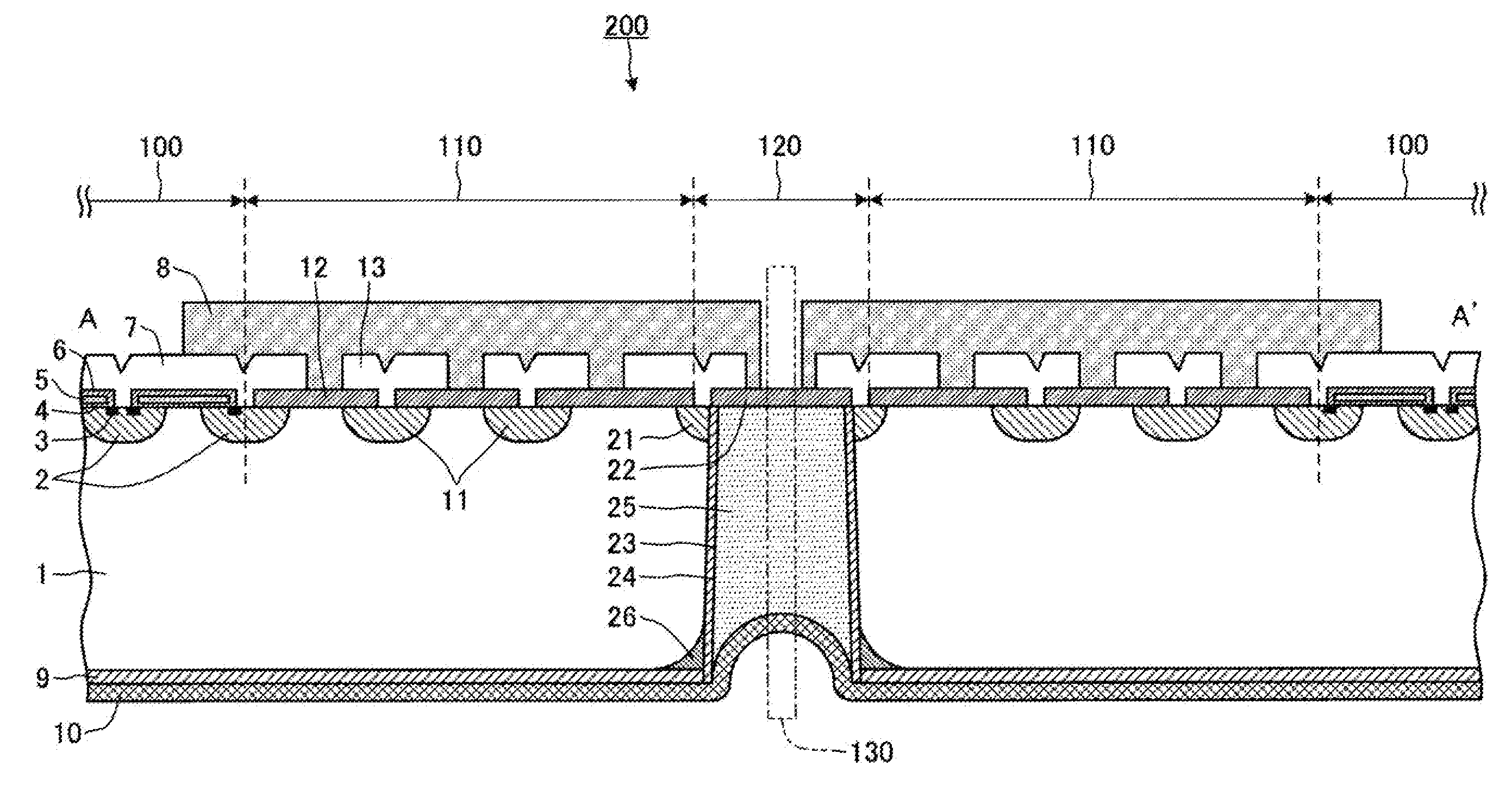
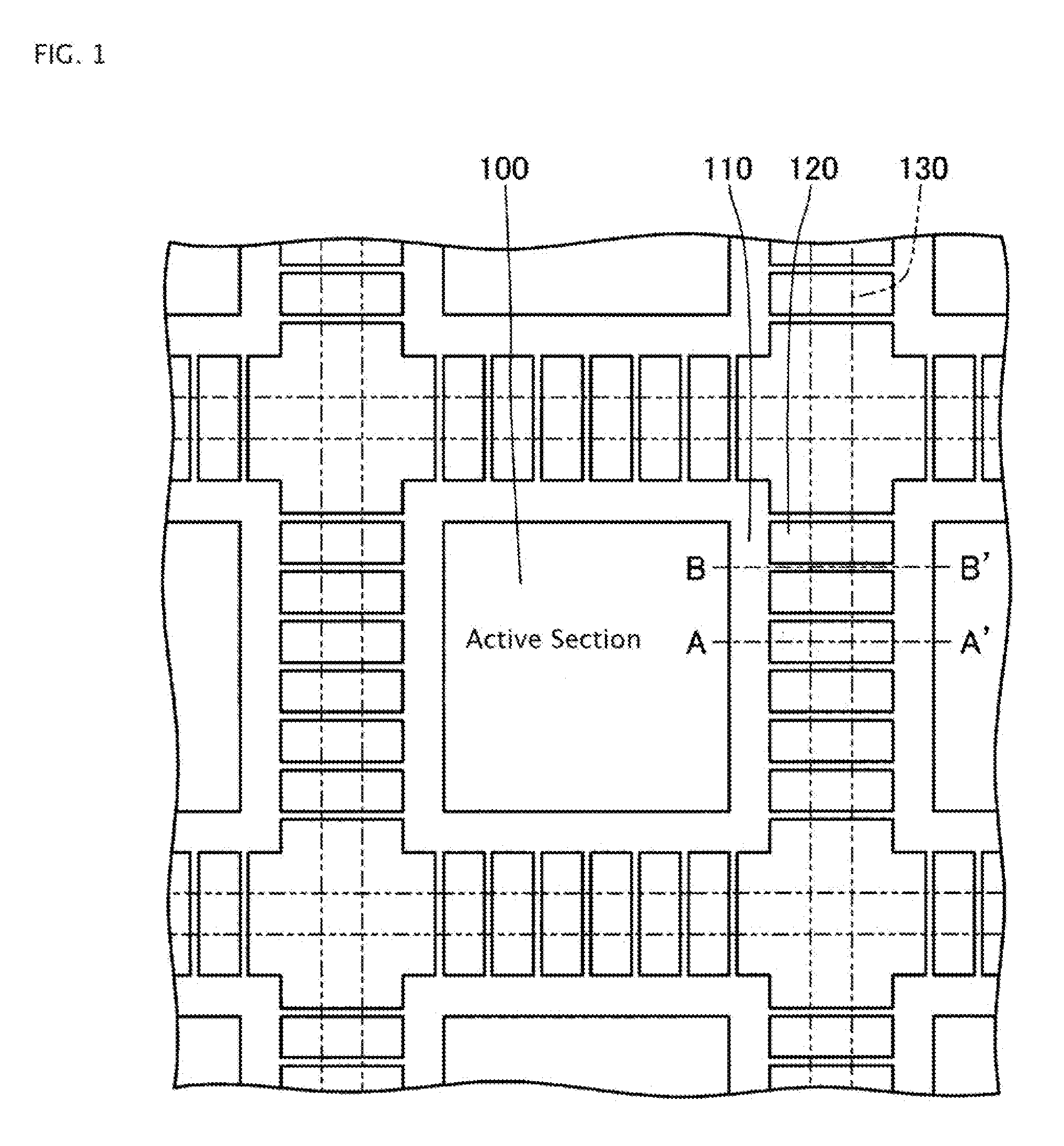
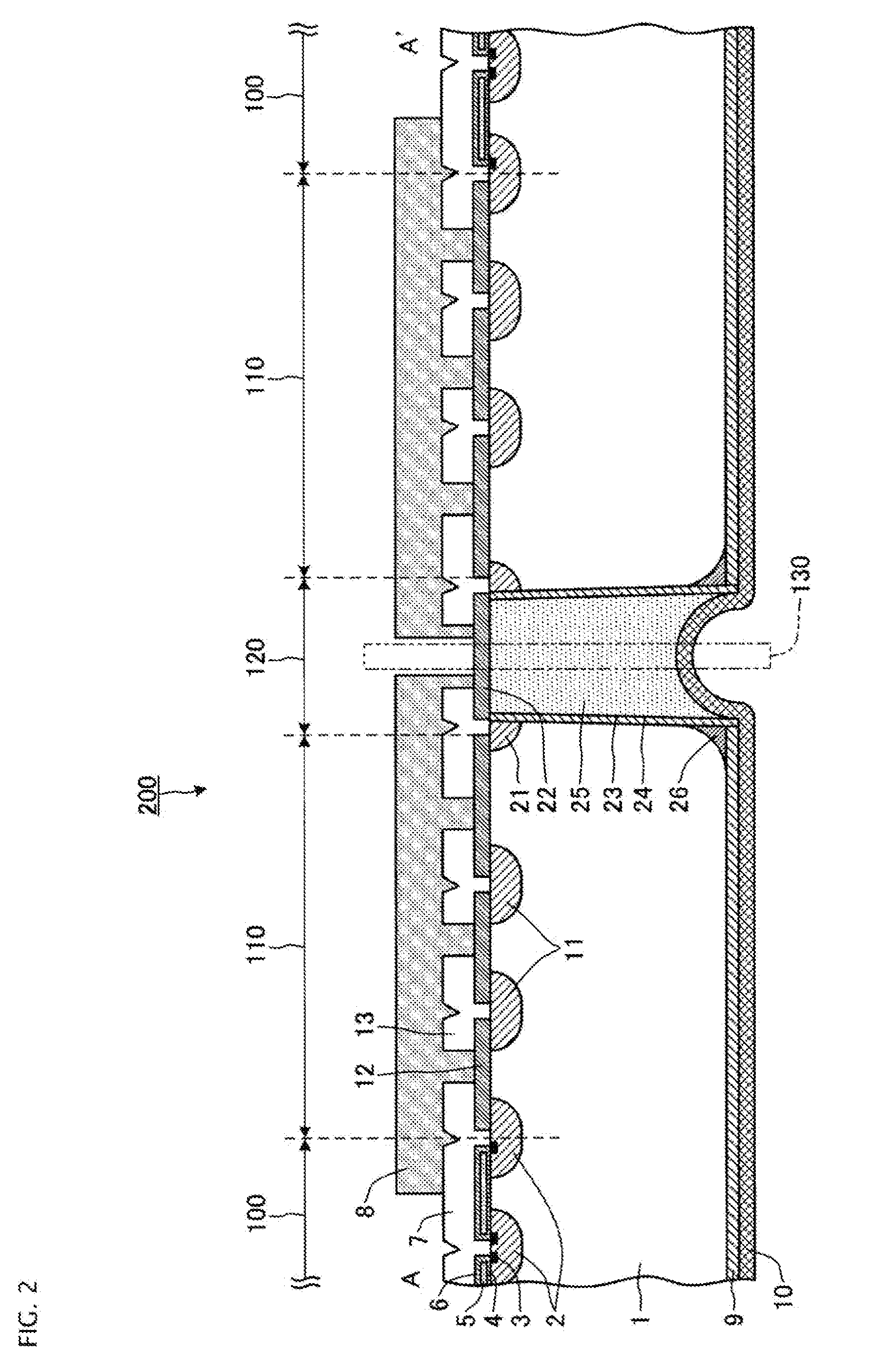
[0094]The structure of a semiconductor device according to a first embodiment of the invention will be described first. FIG. 1 is a top plan view showing the structure of the semiconductor device according to the first embodiment. FIG. 2 is a cross sectional view along the line segment A-A′ in FIG. 1. FIG. 3 is a cross sectional view along the line segment B-B′ in FIG. 1. In FIG. 1, the detailed structures are not described to clearly illustrate active section 100, edge termination section 110 having a voltage blocking structure (hereinafter referred to simply as “edge termination section 110”), and separation section 120 having a device separation structure (hereinafter referred to simply as “separation section 120”).
[0095]As shown in FIG. 1, semiconductor device 200 according to the first embodiment includes active section 100, edge termination section 110 around active section 100, and separation sections 120 scattered around edge termination section 110. Since separation section...
second embodiment
[0105]Now a semiconductor device according to a second embodiment of the invention will be described below. FIG. 4 is a cross sectional view of the semiconductor device according to the second embodiment.
[0106]Semiconductor device 210 according to the second embodiment is manufactured in the following way. A surface device structure is formed on the first major surface side of semiconductor substrate 1 and the back surface side of semiconductor substrate 1 is polished. Then, trench 33 is formed from the first major surface side. Impurity diffusion is conducted from the first major surface side to form p+-type separation region 34. To make it easier to form p+-type separation region 34, an insulator is buried in trench 33 for infill 35. Since the other structures are the same as those in semiconductor device 200 according to the first embodiment, their duplicated descriptions are omitted for the sake of simplicity.
[0107]Any portion of p+-type separation region 34, wider than (or dope...
third embodiment
[0108]Now a semiconductor device according to a third embodiment of the invention will be described below. FIG. 5 is a cross sectional view of the semiconductor device according to the third embodiment.
[0109]As shown in FIG. 5, no insulator is not buried in trench 23 formed from the second major surface side in separation section 122 having a device separation structure (hereinafter referred to simply as “separation section 122”) in semiconductor device 220 according to the third embodiment. Since the other structures are the same as those in semiconductor device 200 according to the first embodiment, their duplicated descriptions are omitted for the sake of simplicity.
[0110]The semiconductor device according to the third embodiment exhibits the same effects as the semiconductor device according to the first embodiment. Since the adjacent chips are connected to each other only with insulation film 22 and collector electrode 10, chips may be isolated from each other without dicing.
PUM
 Abstract
Description
Claims
Application Information