Electronic device and manufacturing method therefor

a manufacturing method and technology for electronic devices, applied in the direction of printed circuit components, sustainable manufacturing/processing, final product manufacturing, etc., can solve the problem of higher cracking risk, and achieve the effect of preventing functional deficiencies and suppressing cracks in electrical connection parts

Active Publication Date: 2011-01-13
RENESAS ELECTRONICS CORP
View PDF13 Cites 22 Cited by
  • Summary
  • Abstract
  • Description
  • Claims
  • Application Information

AI Technical Summary

Benefits of technology

[0039]The present invention gives rise to at least one of the following meritorious effects:
[0040]Even if the stress attributable to the difference between the coefficient of thermal expansion of an electronic element and those of an interposer substrate and an interconnection substrate is applied to a connection part between the interposer substrate and the interconnection substrate, it is possible to suppress a crack in the electrical connection part by making the connection part(s) subjected to the large stress as a dummy connection part(s). It is thus possible to prevent functional deficiencies caused by failure in electrical conduction at the electrical connection part.

Problems solved by technology

Hence, the risk of cracking is higher with the use of the lead-free solder.

Method used


Image

  • Electronic device and manufacturing method therefor
  • Electronic device and manufacturing method therefor
  • Electronic device and manufacturing method therefor

Examples


Embodiment Construction

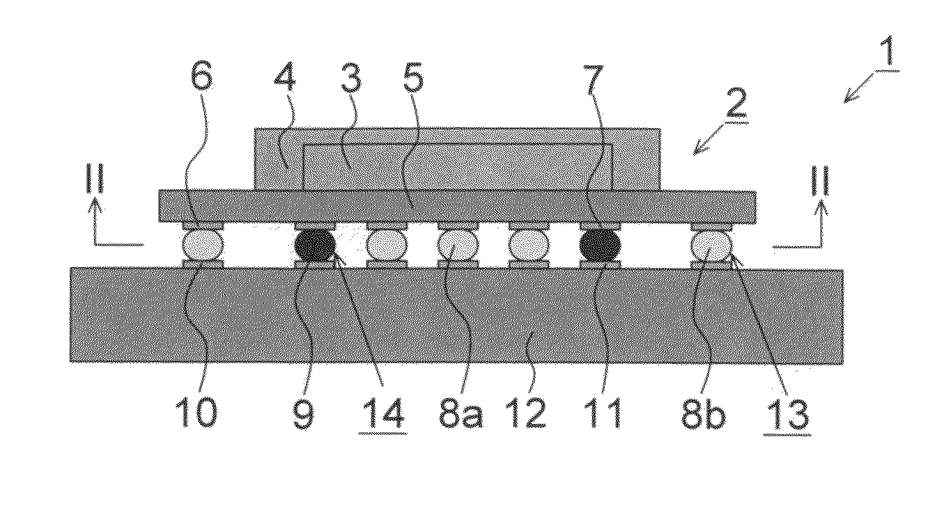
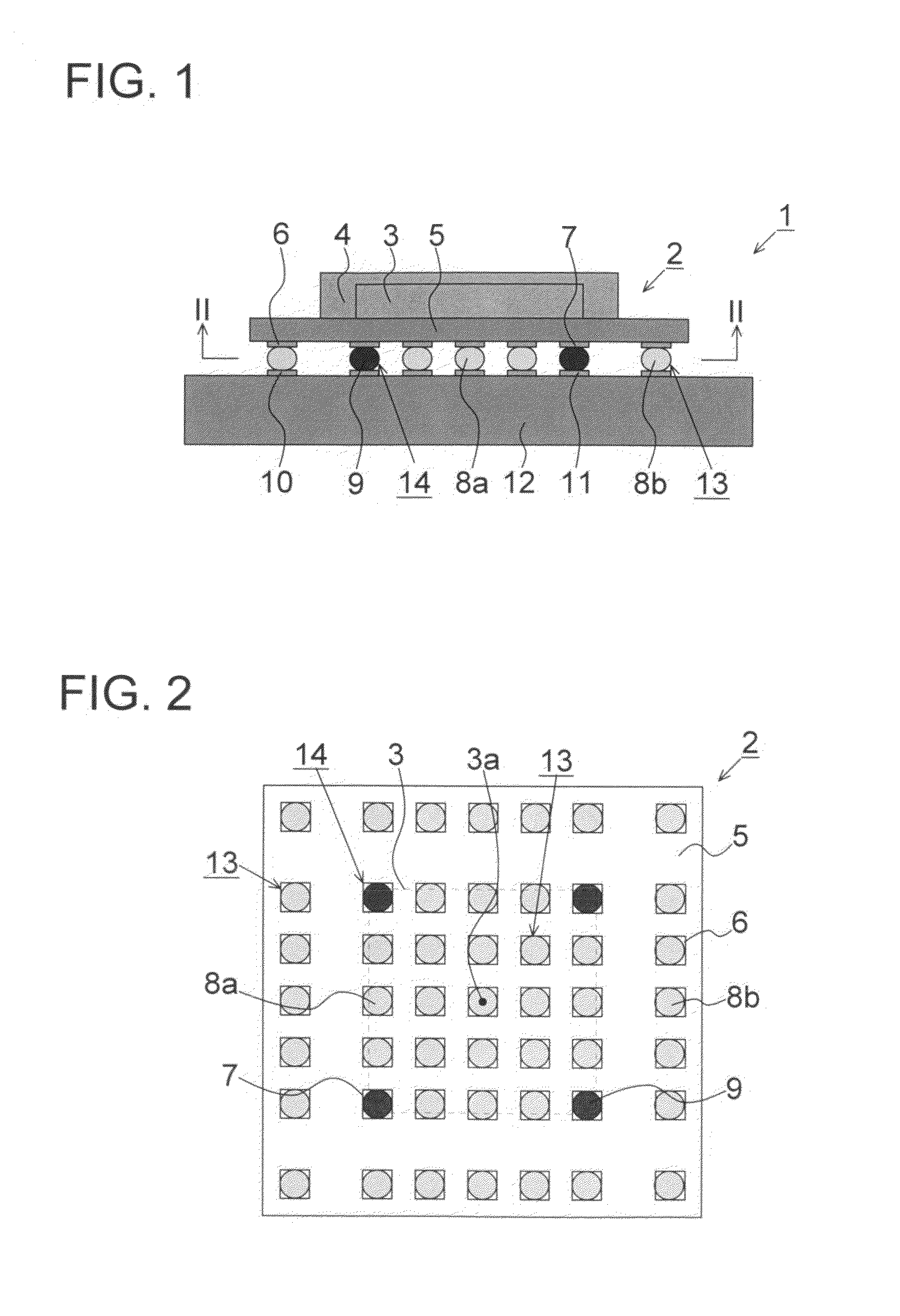
[0080]An electronic device according to a first exemplary embodiment of the present invention will now be described. FIG. 1 shows a schematic cross sectional view of an electronic device according to the first exemplary embodiment of the present invention, and FIG. 2 shows a schematic cross sectional view taken along line II-II of FIG. 1. The electronic device 1 includes an interconnection substrate 12 and an electronic element package 2 mounted on the interconnection substrate 12. The electronic element package 2 includes an interposer substrate 5, an electronic element 3 mounted on one surface of the interposer substrate 5, an encapsulation resin 4 for sealing the electronic element 3, package electrodes for electrical connection 6 provided on the other surface of the interposer substrate 5, and dummy package electrodes 7. There is no particular limitation to the mode of packaging of the electronic element 3 in the electronic element package 2, and flip chip packaging or wire bond...


PUM


Abstract

An electronic device includes the electronic element, the interposer substrate, on one surface of which the electronic element is mounted, and the interconnection substrate, on one surface of which the interposer substrate is mounted. One portion of the connection parts is an electrical connection part that electrically interconnects the interposer substrate and the interconnection substrate. The remaining portion is a dummy connection part that produces no functional deficiency even when the dummy connection part does not electrically interconnect the interposer substrate with the interconnection substrate. The dummy connection part includes at least one of the connection parts that at least partially overlap with the electronic element in a plan projection and are preferably arranged along an outer rim of the plan projection of the electronic element.

Description

REFERENCE TO RELATED APPLICATION[0001]This invention claims the benefits (priority) of JP Patent Application 2008-068034 filed on Mar. 17, 2008, which is hereby incorporated by reference herein in its entirety.TECHNICAL FIELD[0002]This invention relates to an electronic device, such as a semiconductor device, obtained on packaging an electronic element package, for example, a semiconductor package, on an interconnection substrate. The electronic element package is a packaged electronic element, such as a packaged semiconductor chip.BACKGROUND ART[0003]FIG. 12 illustrates a schematic cross sectional view of an electronic device of the background art. An electronic device 81 includes an electronic element package 82 and an interconnection substrate 92. The electronic element package 82 is obtained on mounting an electronic element 83 on an interposer substrate 85 and sealing the resulting assembly with an encapsulation resin 84. The interconnection substrate 92 has mounted thereon the...

Claims


Application Information

Patent Timeline
Patent Type & Authority Applications(United States)
IPC IPC(8): H01L23/52H01L21/50
CPCH01L23/49816H01L23/49838H01L2924/12044H01L2924/15311H05K3/321H05K3/3436H01L2924/0002H05K2201/094H05K2201/09781H01L2924/00Y02P70/50
Inventor KANETAKA, YOSHIFUMI
Owner RENESAS ELECTRONICS CORP
Why Eureka
Try Eureka