Amplifier stage

a technology of amplifier stage and amplifier, which is applied in the direction of amplifiers with field-effect devices, low frequency amplifiers, high frequency amplifiers, etc., can solve the problems of affecting the performance of field-effect transistors, affecting the audio quality at much lower frequencies, and the so-called miller effect, so as to achieve good backward isolation properties and eliminate the miller effect

Inactive Publication Date: 2011-01-13
SONY ERICSSON MOBILE COMM AB
View PDF9 Cites 8 Cited by
  • Summary
  • Abstract
  • Description
  • Claims
  • Application Information

AI Technical Summary

Benefits of technology

[0014]According to another embodiment of the present invention, an amplifier stage for generating an amplified output signal is provided. The amplifier stage provides the amplified output signal at an output terminal of the amplifier stage based on an input signal at an input terminal of the amplifier stage. The amplifier stage comprises a first transistor, a second transistor, a third transistor and a fourth transistor. The first transistor is a field effect transistor (FET) comprising a source terminal, a drain terminal, and a gate terminal. The gate terminal of the first transistor is coupled to the input terminal of the amplifier stage via a first capacitor of the amplifier stage. The gate terminal of the first transistor is furthermore coupled to a first bias voltage via a first bias resistor of the amplifier stage. The second transistor is a bipolar transistor comprising an emitter terminal, a collector terminal, and a base terminal. The emitter terminal of the second transistor is coupled to the drain terminal of the first transistor, and the collector terminal of the second transistor is coupled to the output terminal of the amplifier stage. The third transistor is a p-channel field effect transistor comprising a source terminal, a drain terminal and a gate terminal. The source terminal of the third transistor is coupled to the base terminal of the second transistor via a first diode of the amplifier stage. The drain terminal of the third transistor is coupled to a first supply voltage.
[0015]The gate terminal of the third transistor is coupled to the input terminal of the amplifier stage via a second capacitor of the amplifier stage and coupled to a second bias voltage via a sec

Problems solved by technology

However, active devices, especially field effect transistors, are affected by the so-called Miller effect, an unwanted non-linear type of feedback.
The Mi

Method used


Image

  • Amplifier stage
  • Amplifier stage
  • Amplifier stage

Examples


Embodiment Construction

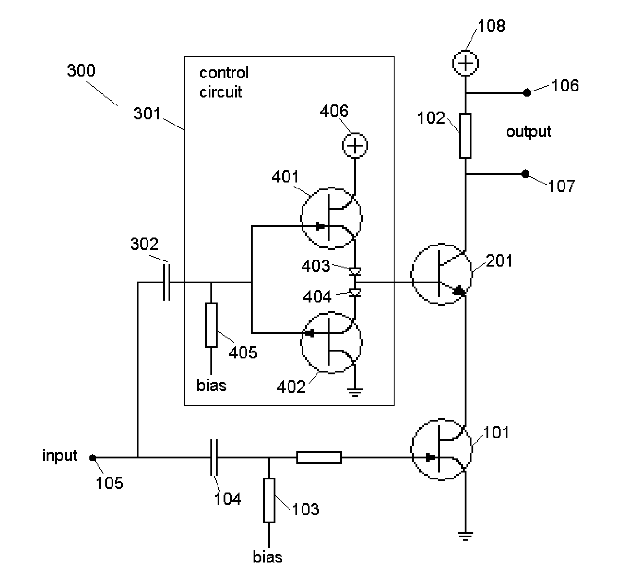
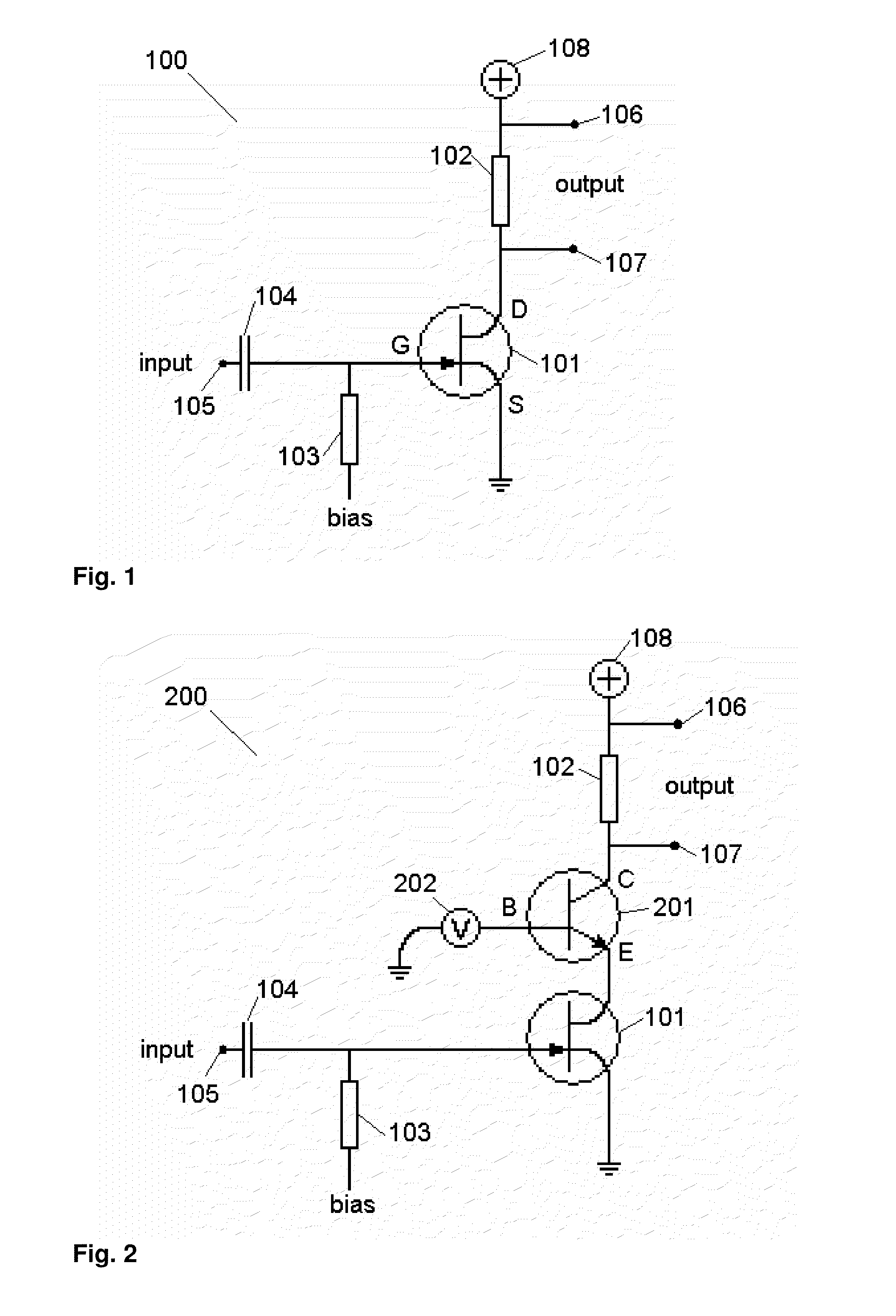
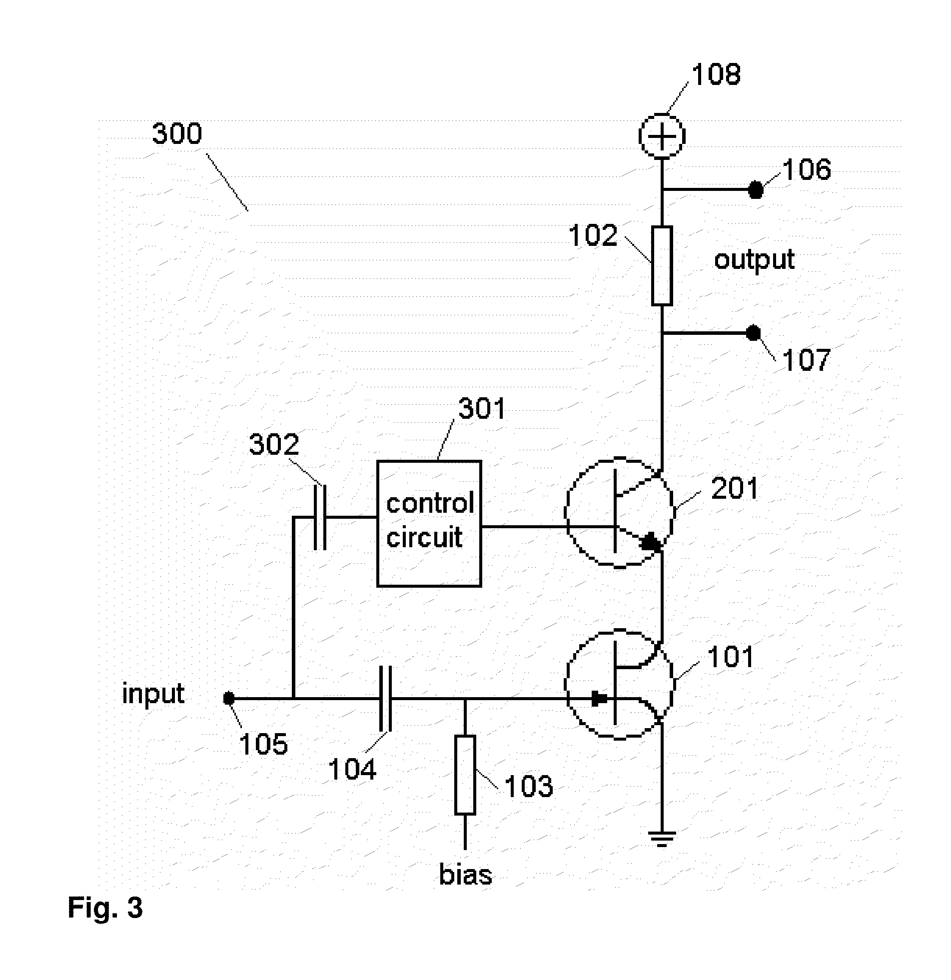
[0026]In the following, exemplary embodiments of the present invention will be described in detail. It is to be understood that the following description is given only for the purpose of illustrating the principles of the invention and it is not to be taken in limiting sense. Rather, the scope of the invention is defined only by the appended claims and is not intended to be limited by the exemplary embodiments hereinafter.

[0027]It is to be understood that in the following detailed description of the embodiment, any direct connection or coupling between functional blocks, devices, components or other physical or functional units shown in the drawings or description herein could also be implemented by an indirect connection or coupling. Same reference signs in the various instances of the drawings refer to similar or identical components.

[0028]It is further to be understood that the features of the various exemplary embodiments described herein may be combined with each other unless s...


PUM


Abstract

An amplifier stage for generating an amplified output signal from an input signal, a mobile device comprising an audio amplifier, and an amplification method for generating an amplified output signal from an input signal using an amplifier stage are described.

Description

BACKGROUND OF THE INVENTION[0001]The present invention relates to an amplifier stage, a mobile device utilizing the amplifier stage as an audio amplifier, and an amplification method using an amplifier stage.BRIEF SUMMARY OF THE INVENTION[0002]According to an embodiment of the present invention, an amplifier stage for generating an amplified output signal at an output terminal of the amplifier stage from an input signal at an input terminal of the amplifier stage is provided. The amplifier stage comprises a first active device, a second active device and a control circuit. The first active device comprises a first terminal, a second terminal, and a control input controlling a current between the first terminal and the second terminal of the first active device. The control input of the first active device is coupled to the input terminal of the amplifier stage. The second active device comprises a first terminal, a second terminal, and a control input controlling a current between t...

Claims


Application Information

Patent Timeline
IPC IPC(8): H03F3/16
CPCH03F1/22H03F3/183H03F3/19H03F2200/552H03F3/423H03F3/426H03F2200/03H03F3/42H03F1/14
Inventor KORNER, HANS PETER
Owner SONY ERICSSON MOBILE COMM AB
Why Eureka
Try Eureka