

Adjustable Interference Filter
- Summary
- Abstract
- Description
- Claims
- Application Information
AI Technical Summary
Benefits of technology
Problems solved by technology
Method used
Image

Examples
Embodiment Construction
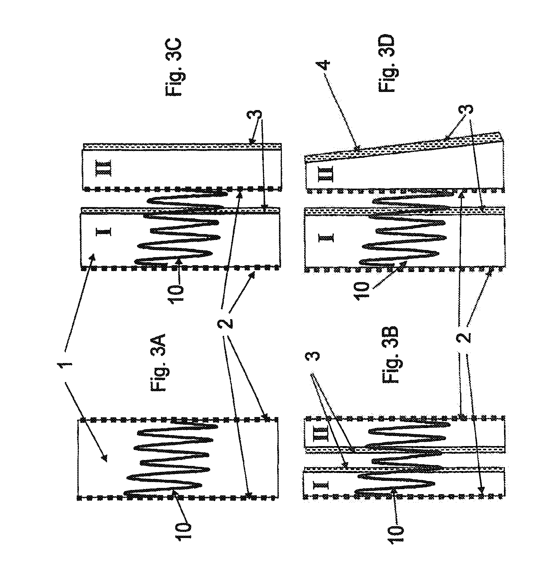
[0028]In FIGS. 3B and 3C an interference filter is illustrated consisting of two silicon discs I,II. The dominating interference of the light 10 oscillating in the filter is between the two transitions 2 between silicon and air. On the other side of the discs an anti reflection layer 3 is position. The result of this is that the interference filter will act like a single silicon disc 1, except for an “invisible” cavity, so that the optical equivalent situation becomes like the one illustrated in FIG. 3A, in which the interference filter is illustrated as a silicon disc 1 with a reflecting surface 2 on both sides. By changing the cavity, meaning the distance between the discs I,II in FIG. 3B, the total optical path length between the reflecting surfaces providing the interference will change. Then the filter may be set in both correlation and anti-correlation modes, so that one achieves the flexibility of an interferometer using cavity and mirrors, at the same time as the advantages ...
PUM
 Abstract
Description
Claims
Application Information