Semiconductor laser device

a laser device and semiconductor technology, applied in semiconductor lasers, instruments, record information storage, etc., can solve the problems of reducing the built-in stress, reducing the manufacturing efficiency, and increasing the cost of the devi

Inactive Publication Date: 2011-01-20
MITSUBISHI ELECTRIC CORP
View PDF2 Cites 10 Cited by
  • Summary
  • Abstract
  • Description
  • Claims
  • Application Information

AI Technical Summary

Benefits of technology

According to the present invention, a semiconductor laser device emitting laser beams with small polarization angles can be obtained without raising costs of a submount.

Problems solved by technology

However, when a light emitting semiconductor device is manufactured according to a configuration of Patent document 1 so as to improve the polarization angle, its manufacturing efficiency is degraded due to the optimized submount's width and thickness, bringing a rising cost problem.
In addition, when AuSn is used as a solder for the submount, similarly to the case of a submount typically used in a conventional light emitting semiconductor device, its eutectic point is a high temperature of 280° C. and therefore, it is unable to sufficiently reduce built-in stress produced between a laser chip and the submount, resulting in an insufficient improvement in polarization angle.

Method used


Image

  • Semiconductor laser device
  • Semiconductor laser device
  • Semiconductor laser device

Examples


embodiment 1

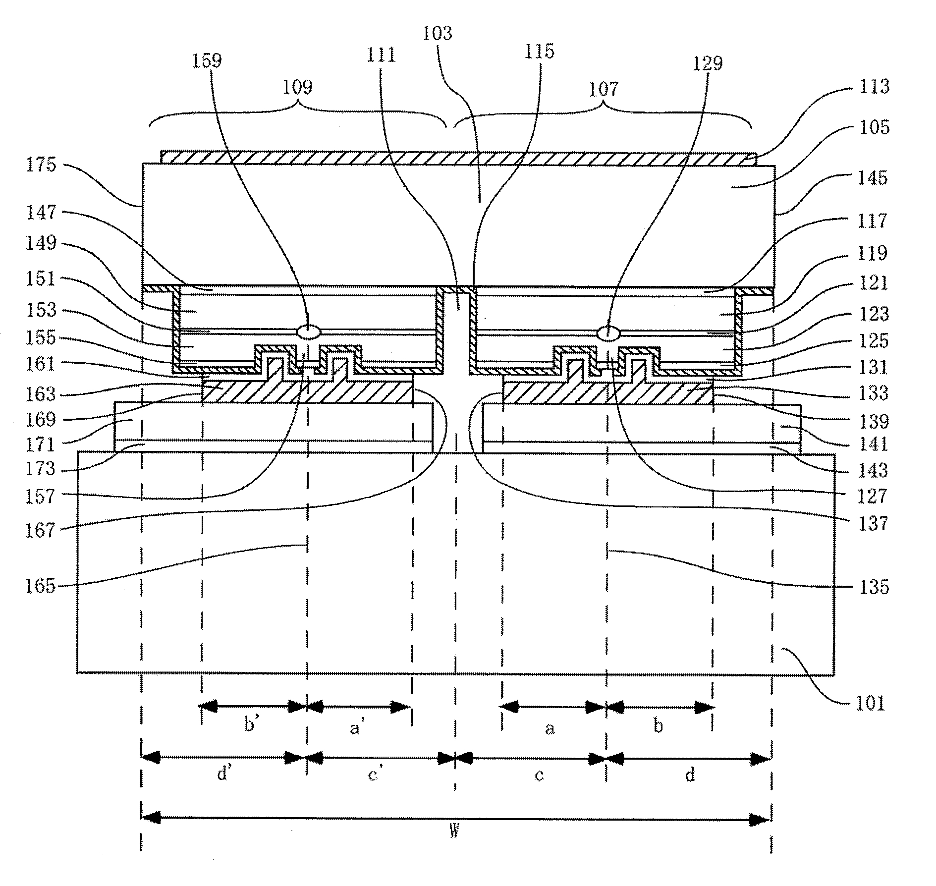
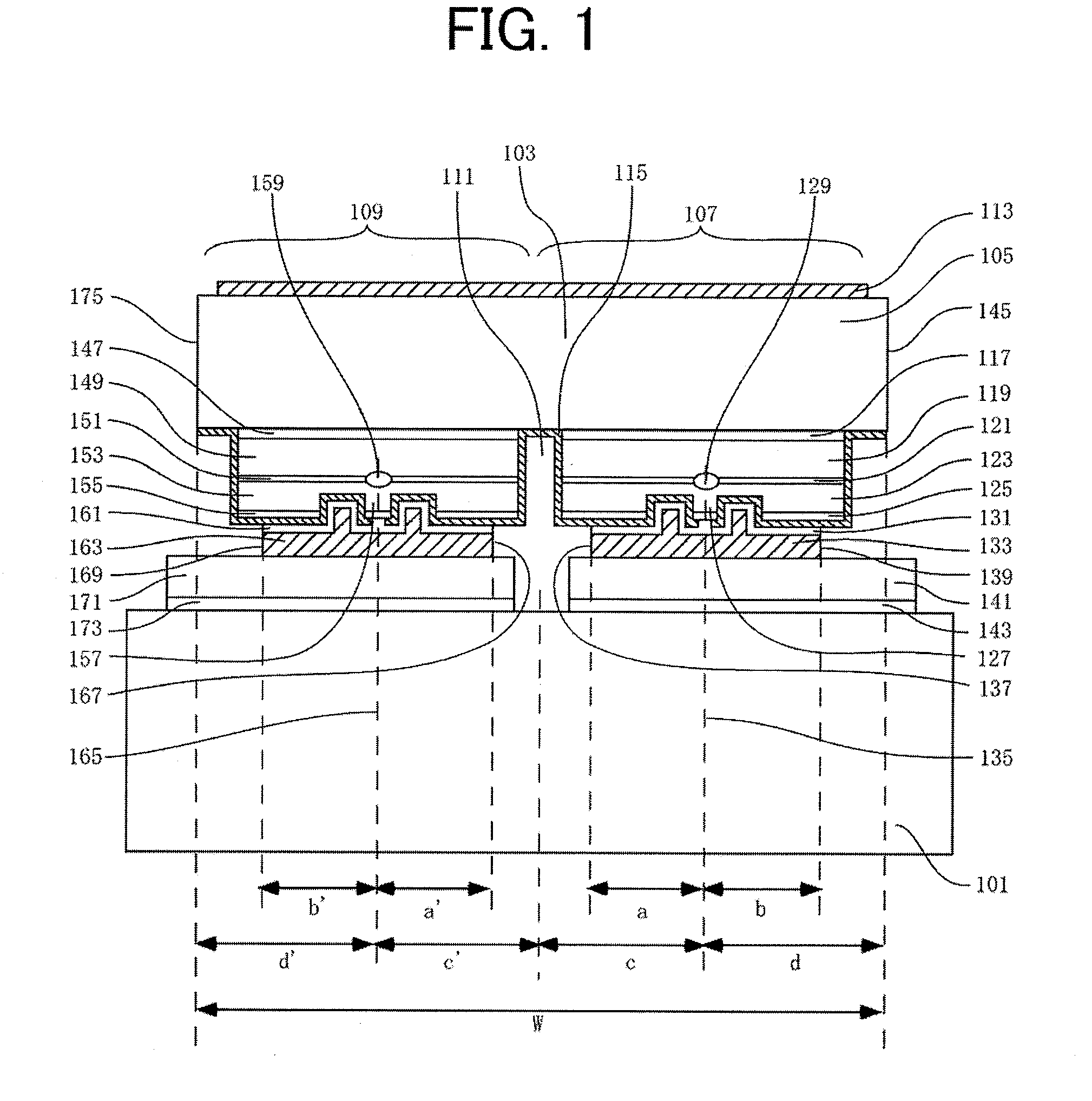
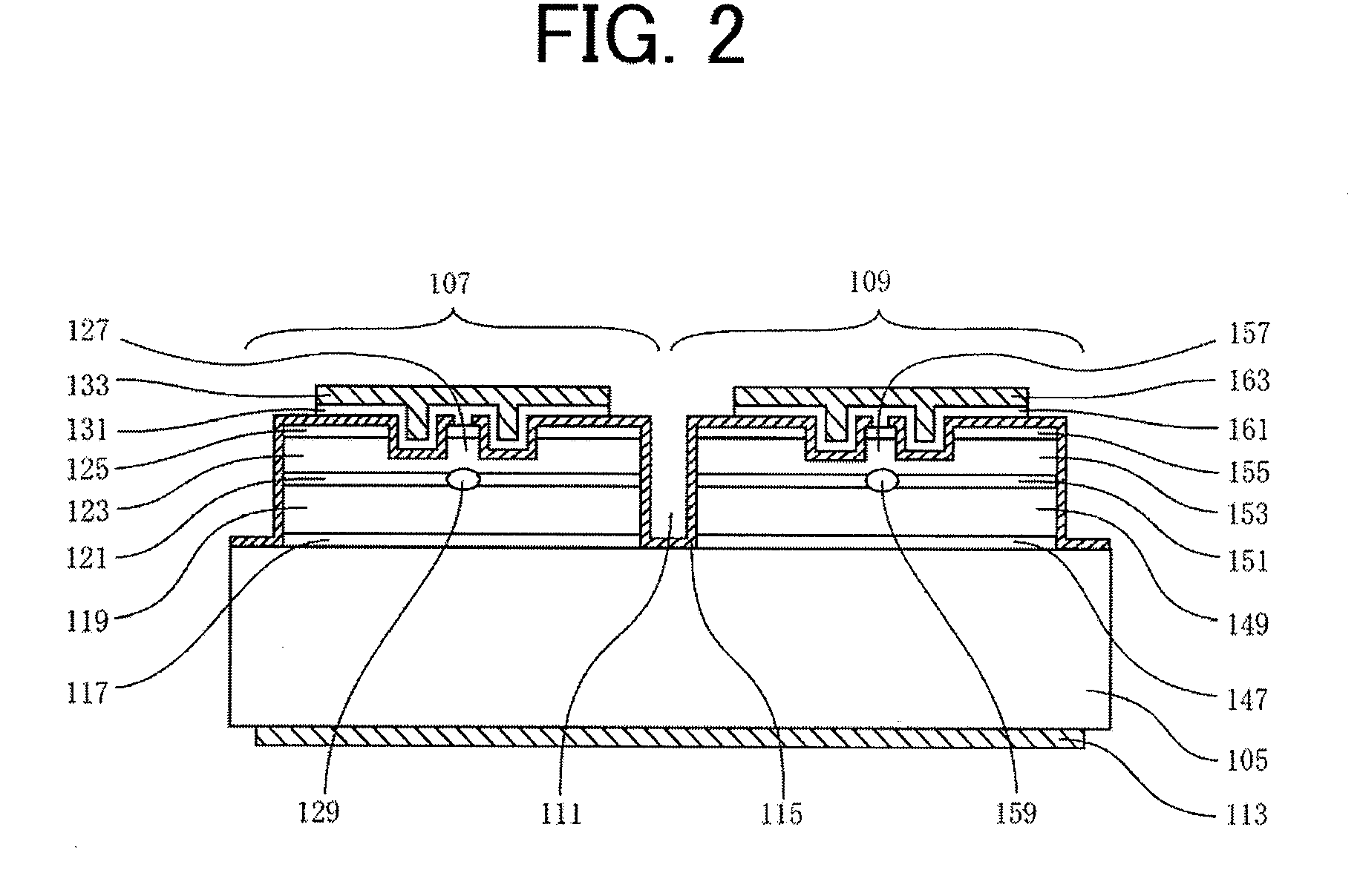
FIG. 1 is a cross-sectional view that illustrates the structure of a semiconductor laser device according to Embodiment 1. FIG. 2 is a cross-sectional view that illustrates the structure of a dual wavelength semiconductor laser chip used in the semiconductor laser device according to Embodiment 1. The semiconductor laser chip 103 is connected onto a submount 101 by junction down. The semiconductor laser chip 103 is a dual wavelength semiconductor laser chip (referred to as a laser chip, below), in which a first semiconductor laser region 107 having a ridge-waveguide for oscillating a 780 nm-wavelength-band laser beam and a second semiconductor laser region 109 having a ridge-waveguide for oscillating a 650 nm-wavelength-band laser beam are monolithically formed on a single n-GaAs substrate 105. In a laser chip 103, in order to electrically insulate the first semiconductor laser region 107 and the second semiconductor laser region 109 from each other, an insulation trench 111 is form...

embodiment 2

FIG. 8 is a cross-sectional view of a dual wavelength semiconductor laser chip used in a semiconductor laser device according to Embodiment 2. The dual wavelength semiconductor laser chip of the semiconductor laser device according to Embodiment 2 includes, on the p-side-electrode platings to be joined to a submount 101, barrier metal layers 801 and 803 made of Ni, Ta, Ti, Pt, Cr, or the like, and Au thin film layers 805 and 807 formed on the barrier metal layers with their thickness of 10 nm to 60 nm to prevent the barrier metals from getting oxidized. The Au thin film layers 805 and 807 may not be formed, if the barrier metal layers 801 and 803 can be prevented from getting oxidized by other methods. By forming the barrier metal layers on the dual wavelength semiconductor laser chip in a manner described above, it is possible to prevent development of depletions (voids) in the vicinity joining surfaces, which would otherwise be produced by mutual diffusion between the electrode ma...


PUM


Abstract

In a semiconductor laser device a dual wavelength semiconductor laser chip is joined onto a submount, junction down, to reduce built-in stress produced between the laser chip and the submount and to decrease polarization angles of the two respective lasers. SnAg solder is used to join the dual wavelength semiconductor laser chip onto the submount. When joining, with respect to each of the two lasers, a ratio of a distance between the center line of a waveguide and an end, placed at a lateral side of the laser chip, of a portion joining the laser chip and the submount, to a distance between the center line of the waveguide and another end, placed toward the center of the laser chip, of the portion joining the laser chip and the submount, falls within a range of 0.69 to 1.46.

Description

BACKGROUND OF THE INVENTION1. Field of the InventionThe present invention relates to a semiconductor laser device, especially a monolithic-dual-wavelength semi-conductor laser device having a ridge-waveguide structure.2. Description of the Prior ArtBecause of development in digital information technology, optical recording media such as DVD-R and CD-R are frequently used. In recent years, a writable optical disc drive compatible with DVD-R, CD-R, and the like is normally installed in a notebook PC as well as a desktop PC. Thus, it is demanded that the optical pick-up—a main component of the writable optical disc drive—be miniaturized, reduced in weight, and reduced in cost, so that efforts are being made to reduce the number of optical components and simplify its manufacturing process. Conventionally, as light source for an optical pick-up compatible with both DVD and CD optical recording methods, two individual semiconductor laser devices, a semiconductor laser device for DVD that ...

Claims


Application Information

Patent Timeline
Patent Type & Authority Applications(United States)
IPC IPC(8): H01S5/22
CPCG11B7/1275G11B2007/0006H01S5/0224H01S2301/14H01S5/22H01S5/4031H01S5/4087H01S5/02272H01S5/0234H01S5/0237
Inventor TAKASE, TADASHITADA, HITOSHIMAEHARA, HIROAKIHISA, YOSHIHIROSAKUMA, HITOSHI
Owner MITSUBISHI ELECTRIC CORP
Why Eureka
Try Eureka