Bonding pad for preventing pad peeling
a bonding pad and peeling technology, applied in the field of semiconductor devices, can solve the problems of ball bonding failure, pad peeling, weakened attachment force of the pad, etc., and achieve the effect of preventing the failure of the bonding pad
- Summary
- Abstract
- Description
- Claims
- Application Information
AI Technical Summary
Benefits of technology
Problems solved by technology
Method used
Image

Examples
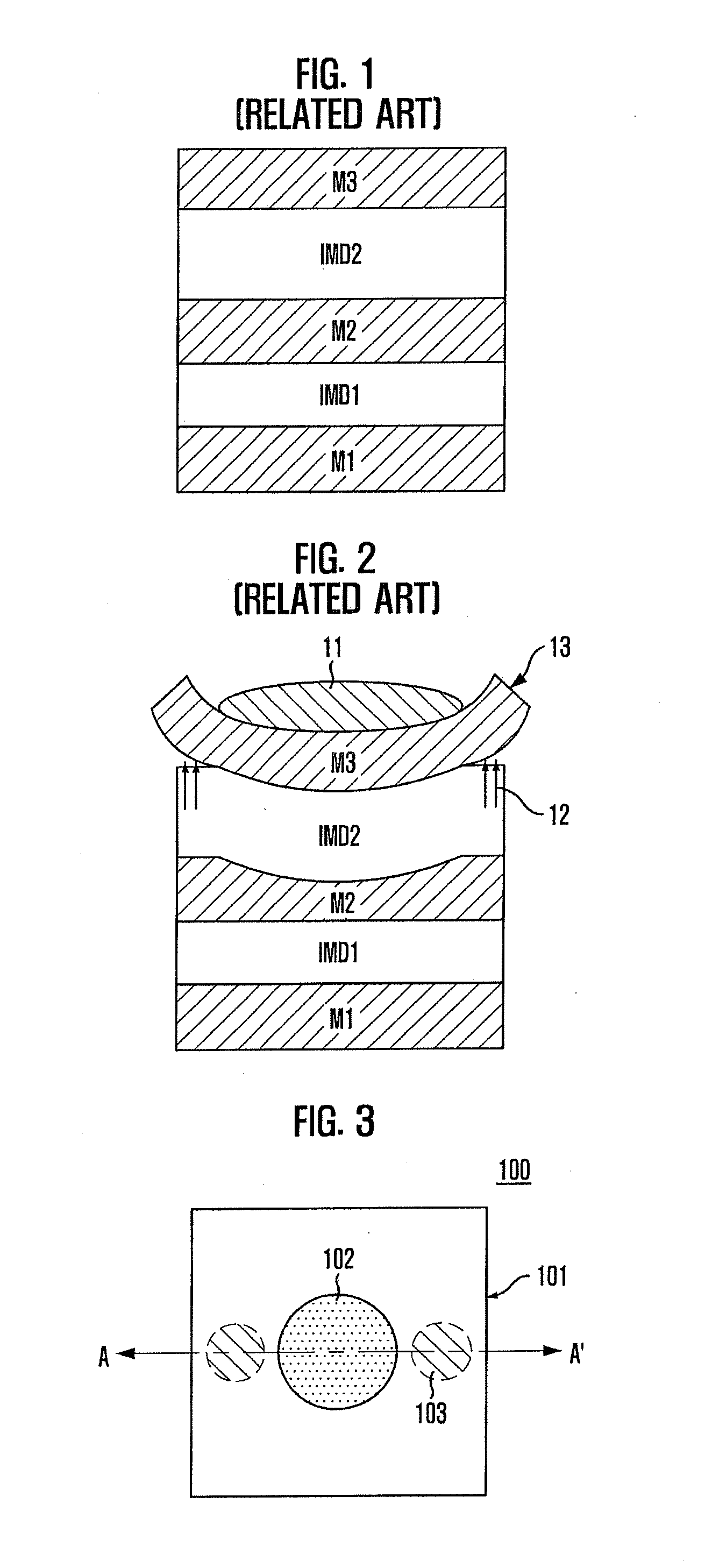
first embodiment
[0035]FIGS. 5A to 5H illustrate cross-sectional views of a method for fabricating a bonding pad in accordance with the present invention.
[0036]Referring to FIG. 5A, a first metal layer 21 is formed and a first insulation layer 22 is formed over the first metal layer 21. The first metal layer 21 may include an aluminum layer or a copper layer, and the first insulation layer 22 may include an intermetal dielectric (IMD), for example, an oxide layer. The first insulation layer 22 is formed of a low-k dielectric, which can reduce a parasitic capacitance between the first metal layer 21 and slits, which will be formed later.
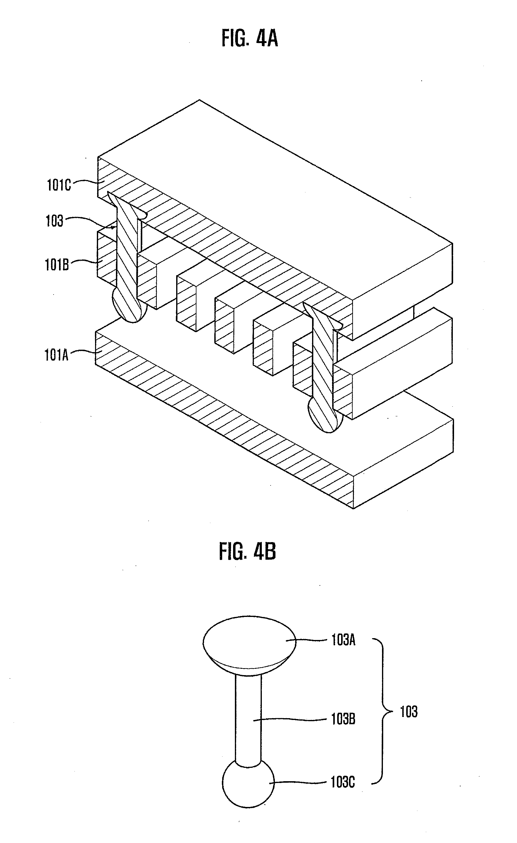
[0037]A plurality of slits 23 formed of the second metal layer is formed over the first insulation layer 22. The plurality of slits 23 are formed by forming the second metal layer and patterning the formed second metal layer so that the patterns are arranged in a slit shape. The plurality of slits 23 has the same size and is arranged with the same spacing. The slits 2...
second embodiment
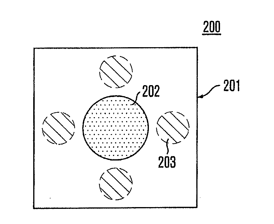
[0055]FIG. 6A illustrates a plan view of a bonding pad in accordance with the present invention. Fixing pins 203 are formed at upper and lower sides of the bonding region 202, as well as at right and left sides of the bonding region 202.
[0056]The bonding pad 200 in accordance with the second embodiment of the present invention includes multiple metal layers 201 and insulation layers (not shown) filled between the multiple layers 201. The fixing pins 203 are coupled between the uppermost metal layer and the underlying metal layers at an outer area outside of a bonding region 202. Although not illustrated, like the first embodiment of the present invention, the multiple metal layers include a first metal layer, a plurality of slits formed of a second metal layer, and a third metal layer. The fixing pins 203 are coupled between the third metal layer and the slits.
[0057]FIG. 6B illustrates a perspective view of the fixing pin in accordance with the second embodiment of the present inven...
third embodiment
[0059]FIG. 6C illustrates a plan view of a bonding pad in accordance with the present invention. A plurality of fixing pins 213 is formed at an outer area of a bonding region 212.
[0060]The bonding pad 210 in accordance with the third embodiment of the present invention includes multiple metal layers 211 and insulation layers (not shown) filled between the multiple layers 211. At least four fixing pins 213 are coupled between the uppermost metal layer and the underlying metal layers at an outer area outside of a bonding region 212. Although not illustrated, like the first embodiment of the present invention, the multiple metal layers include a first metal layer, a plurality of slits formed of a second metal layer, and a third metal layer. The fixing pins 213 are coupled between the third metal layer and the slits.
[0061]Like the first embodiment of the present invention, the bonding pad 210 in accordance with the third embodiment of the present invention can prevent the pad from peeli...
PUM
| Property | Measurement | Unit |
|---|---|---|
| repulsive force | aaaaa | aaaaa |
| attachment force | aaaaa | aaaaa |
| pressure | aaaaa | aaaaa |
Abstract
Description
Claims
Application Information
 - R&D
- Intellectual Property
- Life Sciences
- Materials
- Tech Scout
- Unparalleled Data Quality
- Higher Quality Content
- 60% Fewer Hallucinations
Browse by: Latest US Patents, China's latest patents, Technical Efficacy Thesaurus, Application Domain, Technology Topic, Popular Technical Reports.
© 2025 PatSnap. All rights reserved.Legal|Privacy policy|Modern Slavery Act Transparency Statement|Sitemap|About US| Contact US: help@patsnap.com