Method for manufacturing plasma display panel

Inactive Publication Date: 2011-01-27
PANASONIC CORP
View PDF4 Cites 1 Cited by
  • Summary
  • Abstract
  • Description
  • Claims
  • Application Information

AI Technical Summary

Benefits of technology

[0009]According to the inkjet printing method above, using an ink containing particles of metal or particles of metal oxide allows a transparent electrode to be formed with high dimensional accuracy and little loss of productivity.

Problems solved by technology

However, to form an indium-tin-oxide (ITO) thin film by sputtering, it needs a vacuum device and an exposure device, that is, a large production facility is required.
Besides, the forming process above has a problem of low productivity and high cost.
In the process of forming a discharge gap between transparent electrodes, large variations in distance of a discharge gap due to poor dimensional accuracy in printing a transparent electrode increase variations in discharge characteristics between discharge cells.
This has brought unevenness to the display surface and impaired the quality of image display.
On the other hand, however, an inkjet printing with a size-reduced ink dot increases the time for printing, decreasing productivity.
Increasing the number of nozzles may contribute to increase in productivity; but the distance between adjacent nozzles cannot be decreased without limit.
This has brought a complex and expensive structure to an ink jet printer.

Method used


Image

  • Method for manufacturing plasma display panel
  • Method for manufacturing plasma display panel
  • Method for manufacturing plasma display panel

Examples


Embodiment Construction

[0025]An exemplary embodiment of the present invention is described hereinafter with reference to the accompanying drawings.

An Exemplary Embodiment

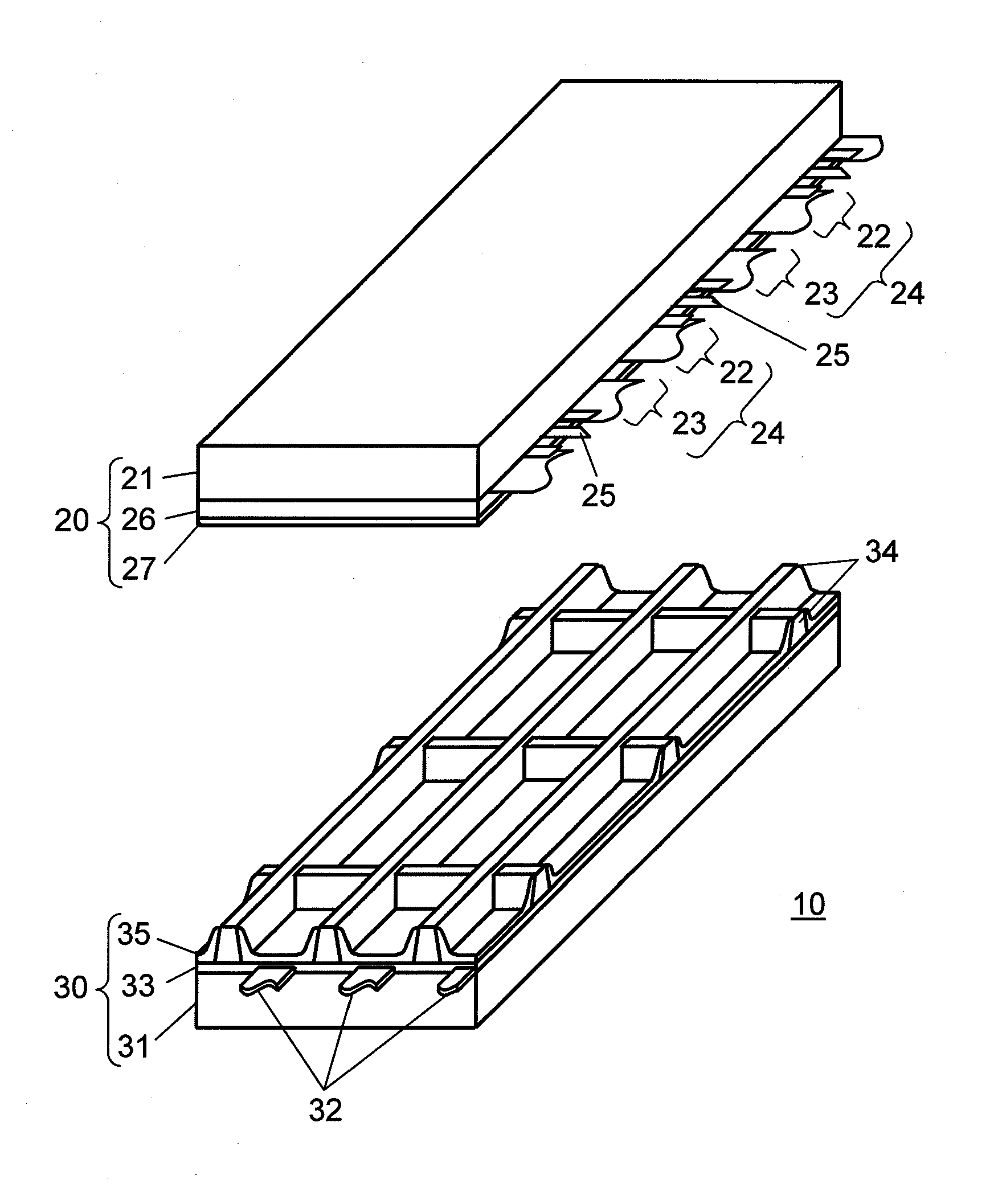
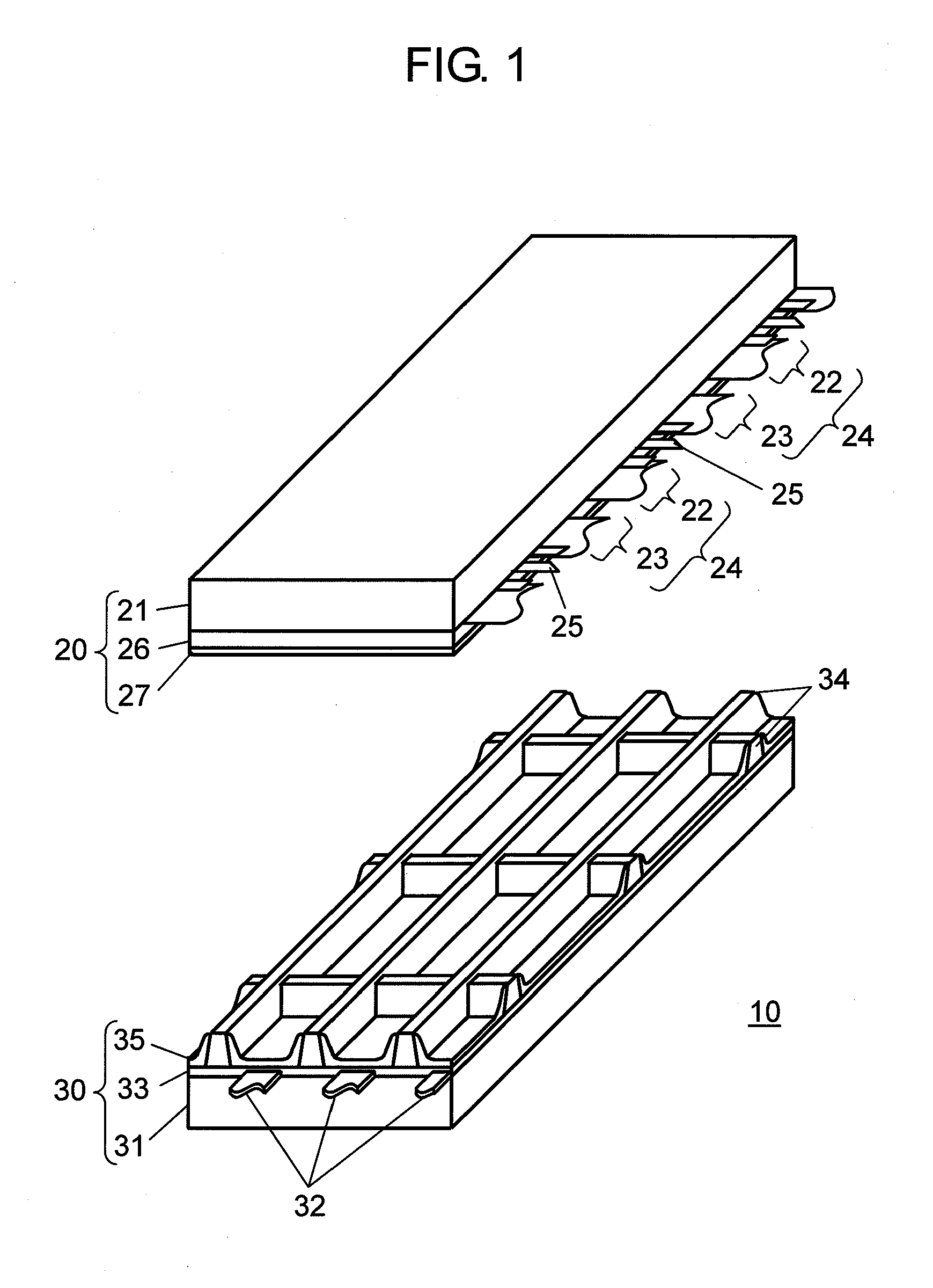
[0026]FIG. 1 is an exploded perspective view showing the structure of the panel in accordance with the first exemplary embodiment of the present invention. Panel 10 has a structure where oppositely disposed front plate 20 and back plate 30 are sealed at the peripheries with sealing material (not shown) and a plurality of discharge cells are formed inside.

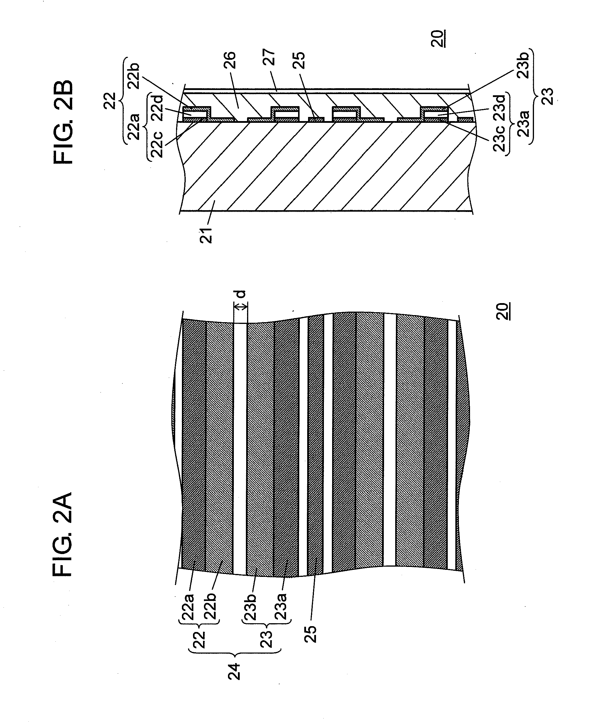
[0027]Front plate 20 has glass-made front substrate 21, display electrode pairs 24 formed of scan electrodes 22 and sustain electrodes 23, black stripes 25, dielectric layer 26, and protective layer 27. On front substrate 21, display electrode pairs 24, each of which is a pair of scan electrode 22 and sustain electrode 23, are formed in parallel with each other. Besides, black stripe 25 is formed between adjacent display electrode pairs 24.

[0028]Although FIG. 1 shows an arrangement of dis...


PUM


Abstract

The present invention provides a method for manufacturing a panel. According to the method, employing an ink containing particles of metal or particles of metal oxide allows transparent electrodes to be formed with high dimensional accuracy and little loss of productivity. Specifically, the transparent electrodes are formed in a manner that an ink containing particles of metal or particles of metal oxide is printed by inkjet printing as a plurality of ink dots with different diameters onto the front substrate.

Description

TECHNICAL FIELD[0001]The present invention relates to a method for manufacturing an AC surface discharge-type plasma display panel used for a display device.BACKGROUND ART[0002]An AC surface discharge-type plasma display panel, which has become dominance in plasma display panel (hereinafter simply referred to as a panel), has a front plate and a back plate oppositely disposed with each other and a plurality of discharge cells therebetween. The front plate has a glass front substrate, display electrode pairs each of which formed of a pair of a scan electrode and a sustain electrode, a dielectric layer and a protective layer that cover them. The back plate has a glass back substrate, data electrodes, a dielectric layer that covers the electrodes, barrier ribs, and phosphor layers. The front plate and the back plate are oppositely disposed and sealed with each other so that the display electrode pairs are located orthogonal to the data electrodes. The discharge space formed between the...

Claims


Application Information

Patent Timeline
IPC IPC(8): B41J2/015H01J9/02H01J11/22H01J11/24H01J11/34
CPCH01J9/02H01J11/24H01J11/12
Inventor MURAKOSO, TOMOHIROHAMADA, RYOTAISHIKURA, YASUHISAURIU, EIICHI
Owner PANASONIC CORP
Why Eureka
Try Eureka