Amplifying circuit, semiconductor integrated circuit, wireless transmission system, and communication apparatus

a technology of semiconductor integrated circuits and amplifiers, applied in the direction of rf amplifiers, amplifiers with semiconductor devices/discharge tubes, rf amplifiers, etc., can solve the problems of high-frequency circuits, 1 involves drawbacks, and inferior frequency characteristics

Active Publication Date: 2011-02-03
SONY CORP
View PDF5 Cites 76 Cited by
  • Summary
  • Abstract
  • Description
  • Claims
  • Application Information

AI Technical Summary

Problems solved by technology

However, the configuration of the high-frequency circuit described in Patent Document 1 involves a drawback due to the fact that the inductor is used in the load circuit (the details thereof will be described in a chapter of “DETAILED DESCRIPTION OF THE PREFERRED EMBODIMENTS”).
However, the differential transimpedance amplifier circuit is configured by using a plurality of transimpedance amplifiers using P-type transistors (such as a PMOS transistor or a PNP transistor) which is inferior in the frequency characteristics to an N-type transistor.
Therefore, the differential transimpedance amplifier circuit involves a drawback in a widening of the broadband.

Method used


Image

  • Amplifying circuit, semiconductor integrated circuit, wireless transmission system, and communication apparatus
  • Amplifying circuit, semiconductor integrated circuit, wireless transmission system, and communication apparatus
  • Amplifying circuit, semiconductor integrated circuit, wireless transmission system, and communication apparatus

Examples


first embodiment

Plurality stage of amplifying cells+Feedback Circuit

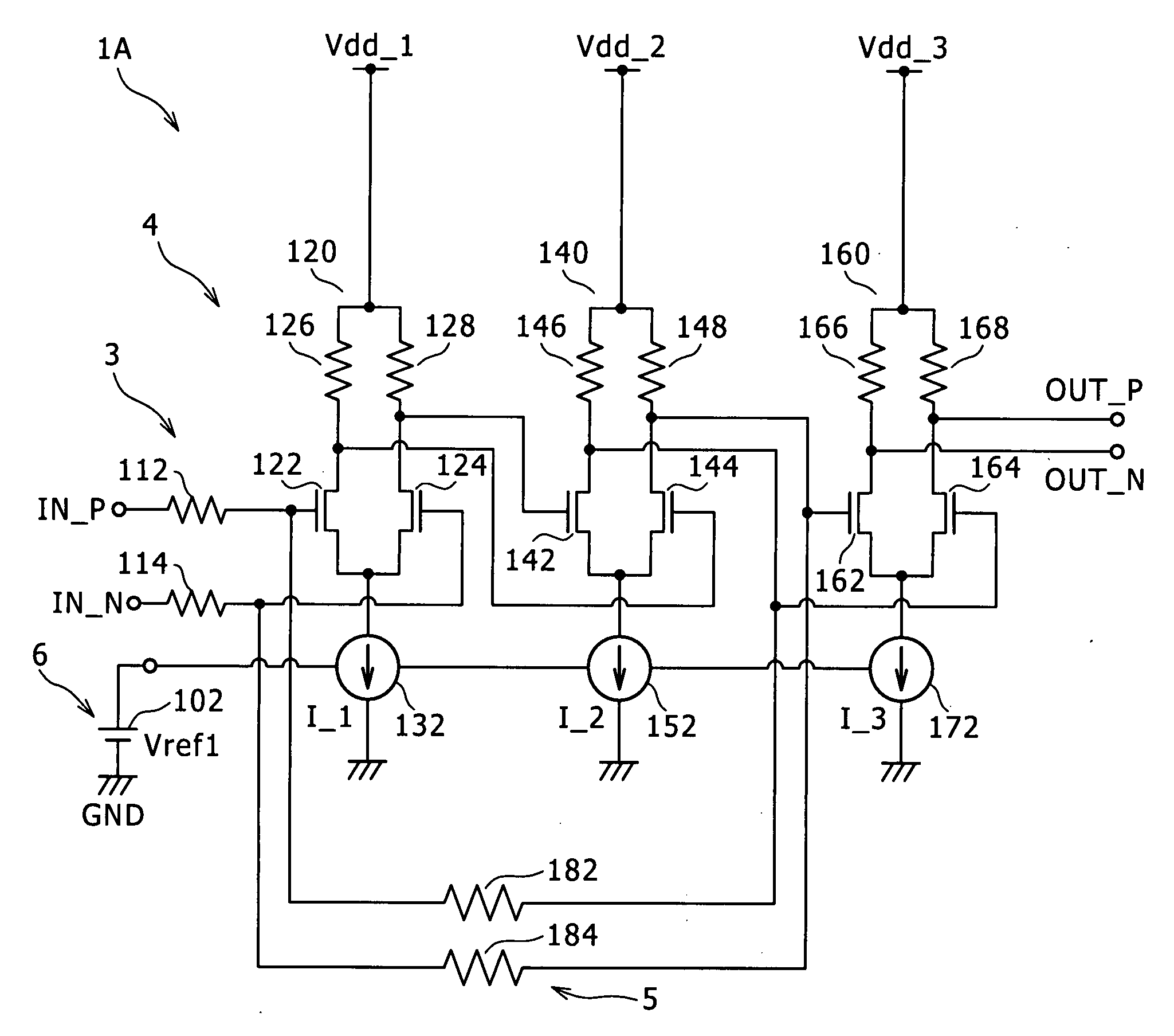
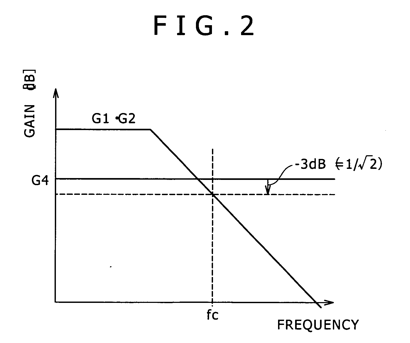
[0035]FIGS. 1 and 2 are respectively a circuit diagram and a graphical representation explaining an amplifying circuit according to a first embodiment of the present invention. Here, FIG. 1 is the circuit diagram showing a configuration of the amplifying circuit according to the first embodiment of the present invention, and FIG. 2 is the graphical representation explaining a frequency band of the amplifying circuit according to the first embodiment of the present invention.

[0036]The amplifying circuit 1A of the first embodiment includes an input portion 3, an amplifying cell portion 4, a D.C. feedback path 5, and a reference power source portion 6. In this case, in the amplifying cell portion 4, a plurality stage of amplifying cells AS each having a function of amplifying a signal are cascade-connected to one another. Also, the reference power source portion 6 generates a reference voltage in accordance with which an operating cur...

second embodiment

First Embodiment+D.C. Operating Point Stabilizing Circuit

[0073]FIG. 3 is a circuit diagram showing a configuration of an amplifying circuit according to a second embodiment of the present invention. The feature of the amplifying circuit 1B according to the second embodiment of the present invention is to include an operating point voltage stabilizing circuit 200 (in other words, a D.C. operating point change suppressing circuit) based on the amplifying circuit 1A of the first embodiment. The operating point voltage stabilizing circuit 200 monitors an operating point voltages of the differential output signals from the amplifying cell AS, and carries out control in such a way that the operating point voltages of the amplifying cells AS are each held constant based on the monitoring result. Hereinafter, the amplifying circuit 1B of the second embodiment will be described by focusing on a difference between the first embodiment and the second embodiment.

[0074]In the amplifying circuit ...

third embodiment

First Embodiment+Load Parasitic Capacitance Correcting Circuit

[0090]FIGS. 4A and 4B are respectively a circuit diagram showing a configuration of an amplifying circuit according to a third embodiment of the present invention, and a circuit diagram showing a configuration of a negative capacitance circuit in the amplifying circuit shown in FIG. 4A. The feature of the amplifying circuit 1C of the third embodiment is to include parasitic capacitance correcting circuits for correcting (canceling) load capacitances which occur parasitically on the output sides of the amplifying cells AS based on the amplifying circuit 1A of the first embodiment. Hereinafter, a description will be given by focusing on a difference from the amplifying circuit 1A of the first embodiment.

[0091]As shown in FIG. 4A, the amplifying circuit 1C of the third embodiment includes negative capacitance circuits 300 each functioning as the parasitic capacitance correcting circuit on the output sides of the amplifying c...


PUM


Abstract

An amplifying circuit includes: an amplifying cell portion configured by cascade-connecting a plurality stage of amplifying cells each including a pair of N-type transistors differentially connected to each other, load resistors and a current source for generating an operating current, and each having a function of amplifying differential signals; a feedback portion configured to feed differential output signals from the amplifying cell in a rear stage side of the amplifying cell portion back to differential input terminals of the amplifying cell on a front stage side; and an input portion configured to supply differential input signals to input terminals in a first stage of the amplifying cell portion.

Description

BACKGROUND OF THE INVENTION[0001]1. Field of the Invention[0002]The present invention relates to an amplifying circuit, a semiconductor integrated circuit having the same mounted thereto, a wireless transmission system having the same mounted thereto, and a communication apparatus having the same mounted thereto. For example, the present invention relates to a high-frequency amplifying circuit which is applied to each of a communication apparatus on a transmission side and a communication apparatus on a reception side each of which operates in an Ultra Wide Band (UWB) or in a millimeter waveband.[0003]2. Description of the Related Art[0004]A broadband amplifying circuit which has flat amplification characteristics in a wide frequency range, for example, is proposed in Japanese Patent Laid-Open Nos. 2009-005137 and 2007-195189 (hereinafter referred to as Patent Documents 1 and 2) as an amplifying circuit which can respond to both requests for a broadband and a large gain.[0005]For ex...

Claims


Application Information

Patent Timeline
Patent Type & Authority Applications(United States)
IPC IPC(8): H03F3/45H04B1/04H04B1/06H04B7/24
CPCH03F3/195H03F2203/45702H03F3/45183H03F3/45659H03F2200/408H03F2200/451H03F2200/78H03F2203/45301H03F2203/45418H03F2203/45424H03F2203/45522H03F2203/45528H03F2203/45631H03F2203/45652H03F3/245
Inventor KOMORI, KENJI
Owner SONY CORP
Why Eureka
Try Eureka