
Method for producing photovoltaic-grade crystalline silicon by addition of doping impurities and photovoltaic cell

a technology of crystalline silicon and impurities, applied in the field of silicon base photovoltaic cells, can solve the problems of high cost, inability to use efficient elimination techniques, and high impact of purification on the total cost of silicon and on its availability on the market, and achieves the effect of convenient implementation

Inactive Publication Date: 2011-02-10
APOLLON SOLAR SAS
View PDF1 Cites 25 Cited by
  • Summary
  • Abstract
  • Description
  • Claims
  • Application Information

AI Technical Summary

Benefits of technology

"The invention provides a method for producing high-quality crystalline silicon with good electrical properties for use in photovoltaic applications. The method involves determining the initial concentrations of doping elements in the silicon feedstock and adding a specific amount of a doping material with low segregation to achieve a desired level of doping in the final product. The resulting silicon has a high conversion efficiency and is cost-effective. The invention also provides a silicon-based solar cell that is economical and efficient."

Problems solved by technology

This method is very efficient for eliminating impurities, but it is extremely costly.
In consequence, the purification has a high impact on the total costs of the silicon and on its availability on the market.
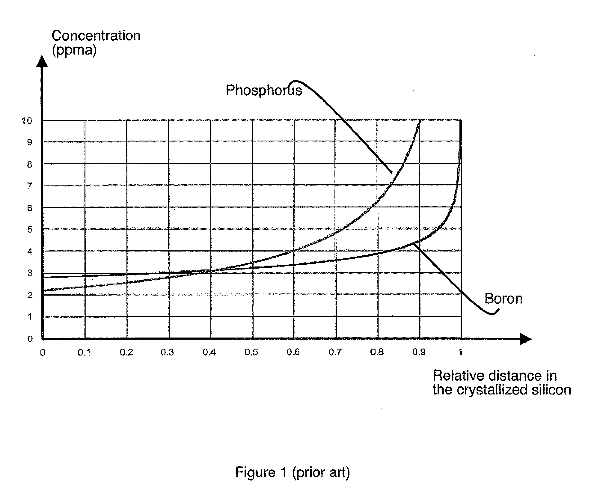
Furthermore, as the doping impurities present relatively high segregation coefficients, this technique cannot be used for efficient elimination of dopants.
Such an ingot presenting different doping types at each of its ends is difficult to manage in a production line.
Such a production method is not satisfactory as it results in too great material losses.

Method used


Image

  • Method for producing photovoltaic-grade crystalline silicon by addition of doping impurities and photovoltaic cell
  • Method for producing photovoltaic-grade crystalline silicon by addition of doping impurities and photovoltaic cell
  • Method for producing photovoltaic-grade crystalline silicon by addition of doping impurities and photovoltaic cell

Examples


Embodiment Construction

[0029]A silicon feedstock is placed in a crucible. The feedstock can be constituted solely of metallurgical grade silicon, of purified metallurgical grade silicon, of photovoltaic grade silicon or of microelectronic grade silicon or of silicon rejects of the latter two lines, for example solar grade or highly-doped electronic grade silicon. The feedstock can also be comprised of a mixture of two or more of these types of silicon.

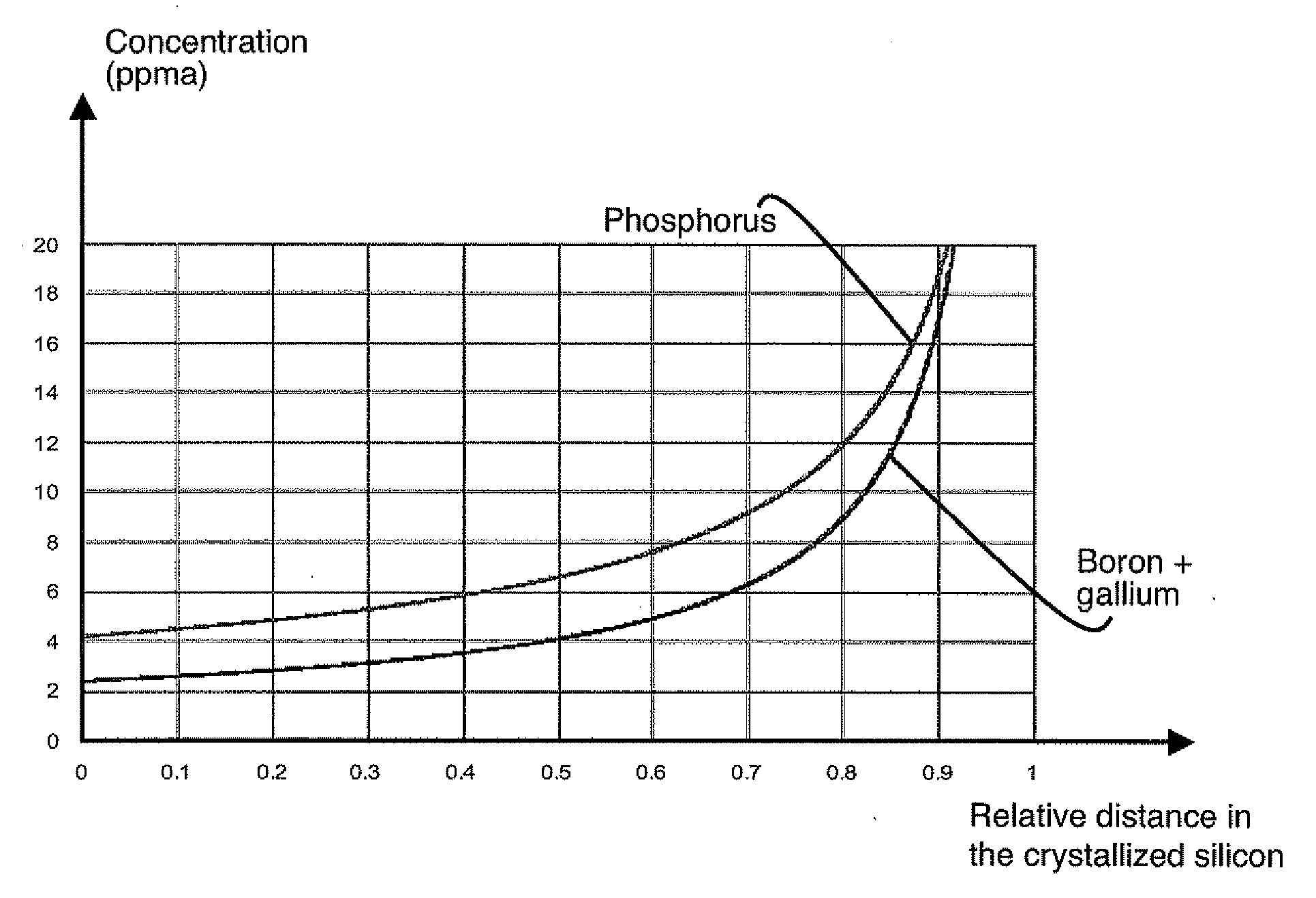
[0030]The sum of the initial concentrations of donor and acceptor type dopant materials present in the raw feedstock is larger than or equal to 0.1 atomic ppm (ppma). Each type of dopant, donor and acceptor, further has a maximum concentration of less than 25 ppma. For example, if the feedstock is essentially constituted by metallurgical grade silicon, the donor and acceptor doping atom concentrations are both comprised between 0.1 and 25 ppma. On the contrary, in another example, if the feedstock is essentially constituted by electronic grade silicon but th...


PUM

PropertyMeasurementUnit
concentrationaaaaaaaaaa
concentrationsaaaaaaaaaa
phosphorus concentrationaaaaaaaaaa

Abstract

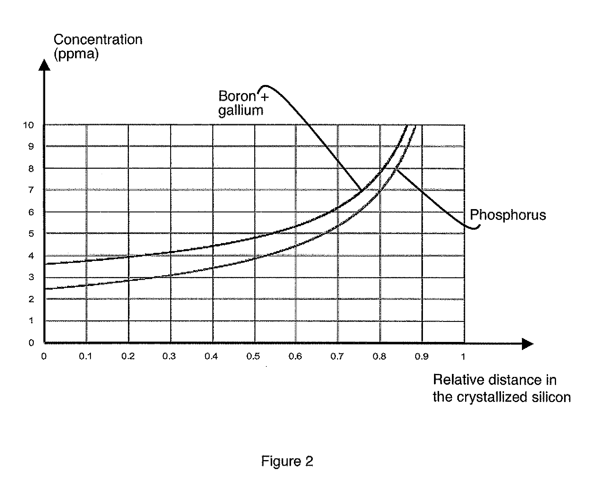
Production of photovoltaic grade crystalline silicon is achieved by crystallization of a molten silicon feedstock, the sum of the initial donor doping element and acceptor doping element concentrations whereof is greater than 0.1 ppma, and both the acceptor and donor doping element concentrations whereof are less than 25 ppma. At least a predefined quantity of a doping material having a segregation coefficient of less than 0.1 is added to the feedstock. This addition enables a crystallized silicon to be produced the difference between the donor and acceptor doping profiles whereof is comprised between 0.1 and 5 ppma over at least 50% of the solidified silicon. A silicon presenting a concentration of at least one of the dopants is greater than or equal to 5 ppma and a difference less than or equal to 5 ppma between these two types of dopant is integrated in a photovoltaic cell.

Description

BACKGROUND OF THE INVENTION[0001]The invention relates to a silicon-base photovoltaic cell.[0002]The invention also relates to a method for producing photovoltaic grade crystalline silicon by crystallizing a molten silicon feedstock.STATE OF THE ART[0003]In conventional manner, silicon used in the photovoltaic industry has to meet a certain number of criteria, in particular in terms of purity, i.e. concentrations of doping and metallic impurities that have to be lower than predefined thresholds. Photovoltaic grade silicon is conventionally obtained in the same way as electronic grade silicon from a metallurgical grade silicon that is purified (via its gas phase) by gaseous means. This method is very efficient for eliminating impurities, but it is extremely costly. In consequence, the purification has a high impact on the total costs of the silicon and on its availability on the market.[0004]New techniques are therefore being looked into to reduce the production cost of silicon able ...

Claims


Application Information

Patent Timeline
Patent Type & Authority Applications(United States)
IPC IPC(8): H01L31/0272H01L31/18
CPCC30B11/00C30B13/00C30B15/04Y02E10/547H01L31/028H01L31/1804Y02E10/52C30B29/06Y02P70/50
Inventor KRAIEM, JEDEINHAUS, ROLANDLAUVRAY, HUBERT
Owner APOLLON SOLAR SAS
Learn More