Tamper-resistant electronic circuit and module incorporating electrically conductive nano-structures

a technology of electrically conductive nano-structures and electronic circuits, which is applied in the direction of emergency protective arrangements for limiting excess voltage/current, instruments, and semiconductor/solid-state device details, etc., can solve the problem of difficult or impossible reverse engineering of protected circuits without complex test equipmen

Inactive Publication Date: 2011-02-10
PFG IP +1
View PDF21 Cites 35 Cited by
  • Summary
  • Abstract
  • Description
  • Claims
  • Application Information

AI Technical Summary

Problems solved by technology

In view of the above, making the reverse engineering of a protected circuit difficult or impossible without complex test equipment is needed.

Method used


Image

  • Tamper-resistant electronic circuit and module incorporating electrically conductive nano-structures
  • Tamper-resistant electronic circuit and module incorporating electrically conductive nano-structures
  • Tamper-resistant electronic circuit and module incorporating electrically conductive nano-structures

Examples


Embodiment Construction

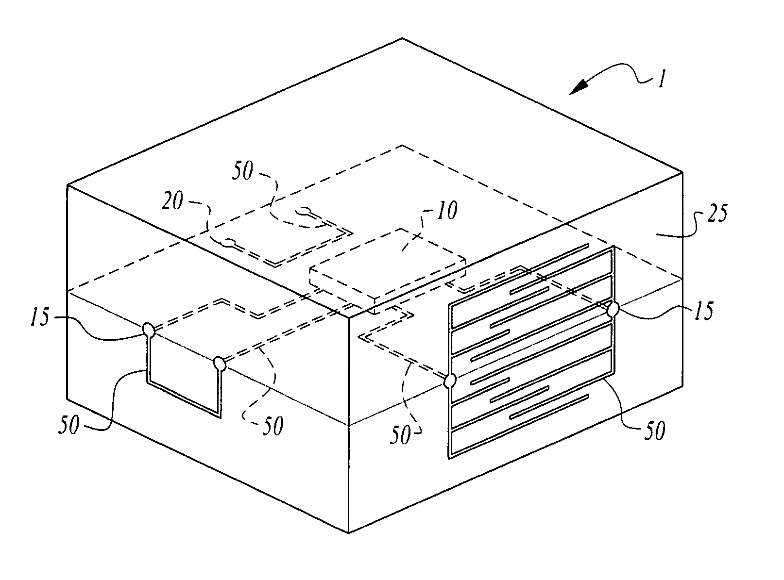
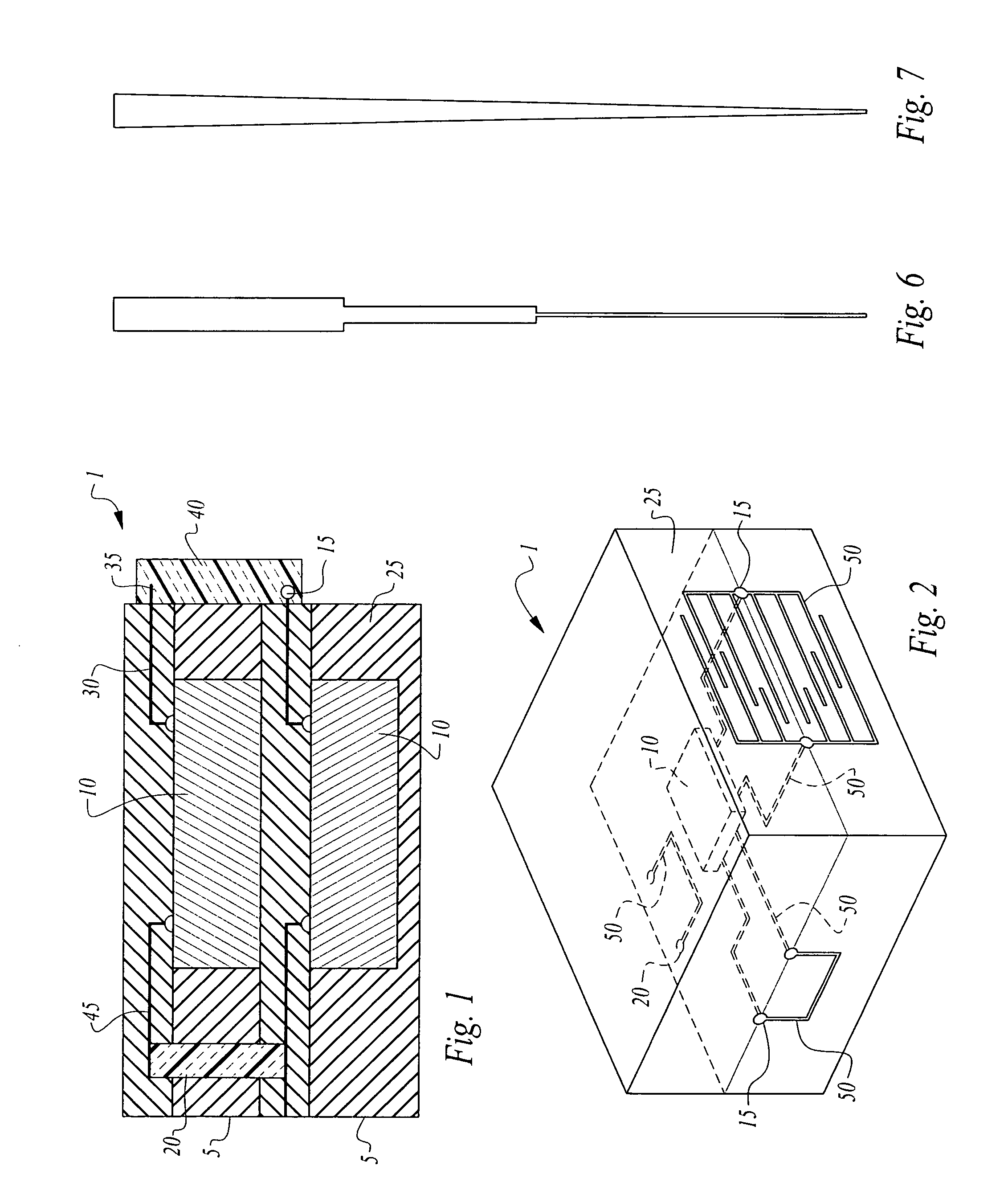
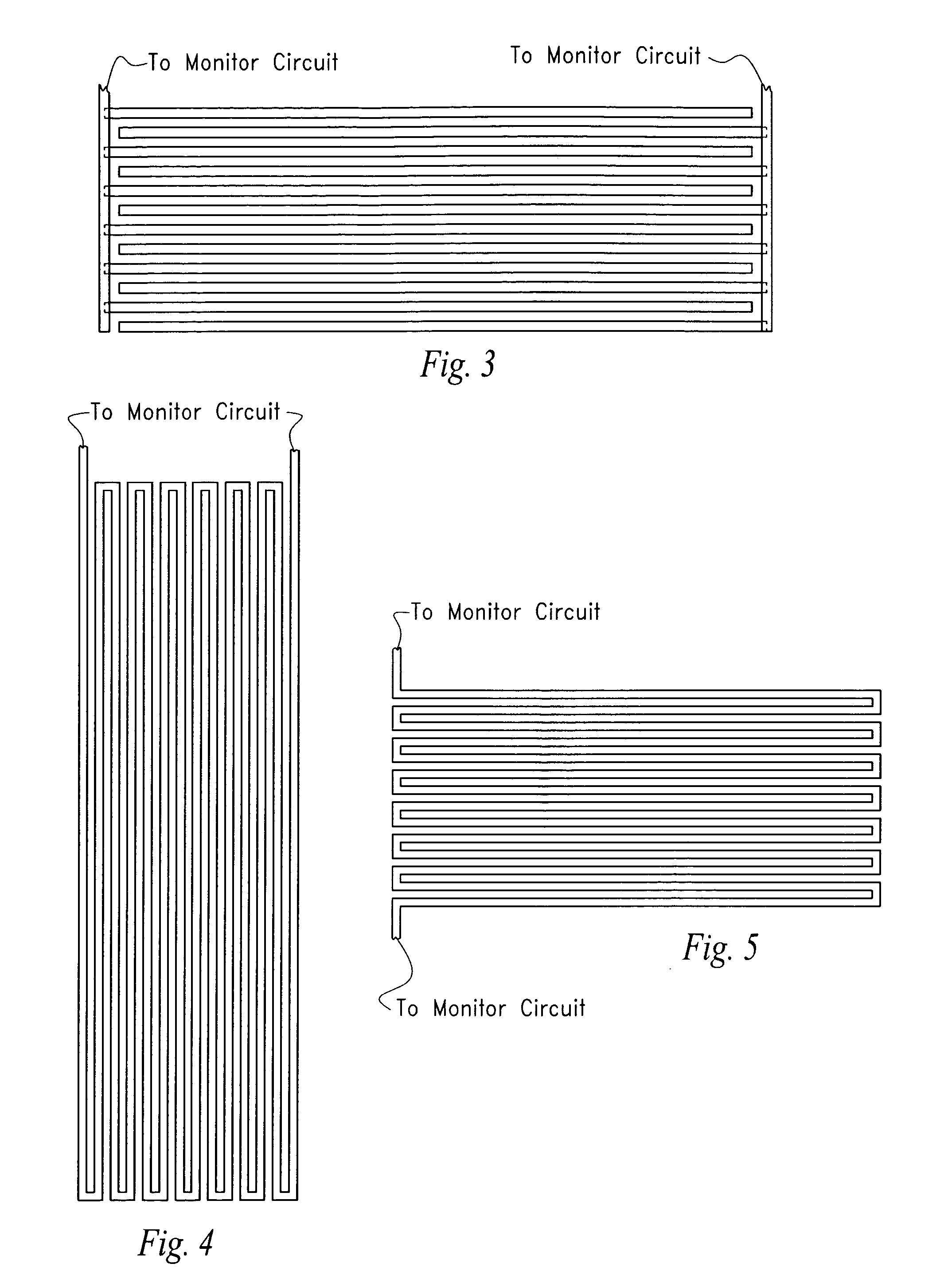
[0022]Stacked microelectronic modules comprised of layers containing integrated circuitry are desirable in that the three-dimensional structure provides increased circuit density per unit area. The elements in a module are generally arranged in a stacked configuration and may comprise stacked silicon die, stacked prepackaged integrated circuit packages, stacked modified prepackaged integrated circuit or stacked neo-layers such as are disclosed in the various U.S. patents below.

[0023]The patents below disclose inventions wherein layers containing integrated circuits chips are stacked and interconnected using any of a number of stacking techniques known to those skilled in the art. For example, Irvine Sensors Corporation, assignee of the instant application, has developed several patented techniques for stacking and interconnecting multiple integrated circuits. Some of these techniques are disclosed in U.S. Pat. Nos. 4,525,921; 4,551,629; 4,646,128; 4,706,166; 5,104,820; 5,347,428; 5,...


PUM


Abstract

A device and method are disclosed comprising one or more electrically conductive nano-structures defined on one or more surfaces of a microelectronic circuit such as an integrated circuit die, microelectronic circuit package (such as a TSOP, BGA or other prepackaged IC) a stacked microelectronic circuit package, or on the surface of one or more layers in a stack of layers containing one or more ICs.In one embodiment, the electrically conductive nano-structure is in electrical connection with a monitoring circuit and acts as a “trip wire” to detect unauthorized tampering with the device or module. Such a monitoring circuit may include a power source such as an in-circuit or in-module battery and a “zeroization” circuit within the chip or package to erase the contents of a memory when the electrically conductive nano-structure is breached or altered. The device may be configured to blow one or more fuses or overcurrent protection devices when the electrically conductive nano-structure is breached or altered.In a further embodiment, one or more electrically conductive nano-structures are used to interconnect and reroute one or more electrical connections between one or more ICs (or dummy leads and vias) to create an “invisible” set of electrical connections on the chip or stack to obfuscate an attempt to reverse engineer the device, i.e., a set of connections that cannot be observed by standard test means such as by X-ray or conventional microscope.

Description

CROSS-REFERENCE TO RELATED APPLICATIONS[0001]This application claims the benefit of U.S. Provisional Patent Application No. 61 / 273,573, filed on Aug. 6, 2010 entitled “Anti Tamper Device with Zeroization Nano Structure” pursuant to 35 USC 119, which application is incorporated fully herein by reference.STATEMENT REGARDING FEDERALLY SPONSORED RESEARCH AND DEVELOPMENT[0002]N / ADESCRIPTION[0003]1. Field of the Invention[0004]The invention relates generally to the field of electronic packages comprising one or more tamper-resistant features. More specifically, the invention relates to the use of electrically conductive nano-structures for the monitoring and protection of an electronic circuit.[0005]2. Background of the Invention[0006]It is a known concern of military and commercial entities that reverse engineering and evaluation of an electronic circuit can occur when such an electronic device (e.g., a microelectronic circuit) falls in to enemy hands or into the possession of a business...

Claims


Application Information

Patent Timeline
Patent Type & Authority Applications(United States)
IPC IPC(8): G01R27/28H02H3/08H05K7/00
CPCH01L23/576H01L25/0657H01L2225/06517H01L2225/06527H01L2225/06541H01L2924/0002H01L2924/3011H01L2924/00
Inventor LEON, JOHNYAMAGUCHI, JAMESOZGUZ, VOLKANBOYD, W. ERIC
Owner PFG IP
Why Eureka
Try Eureka