

Voltage variation reducing circuit and semiconductor device using the same
a voltage variation and circuit technology, applied in the direction of voltage/current interference elimination, reliability increasing modifications, instruments, etc., can solve the problems of power source noise that cannot be reduced power source noise cannot be voltage-dependent, etc., to reduce the variation of a power source voltage, reduce the voltage variation, the effect of increasing the circuit area
- Summary
- Abstract
- Description
- Claims
- Application Information
AI Technical Summary
Benefits of technology
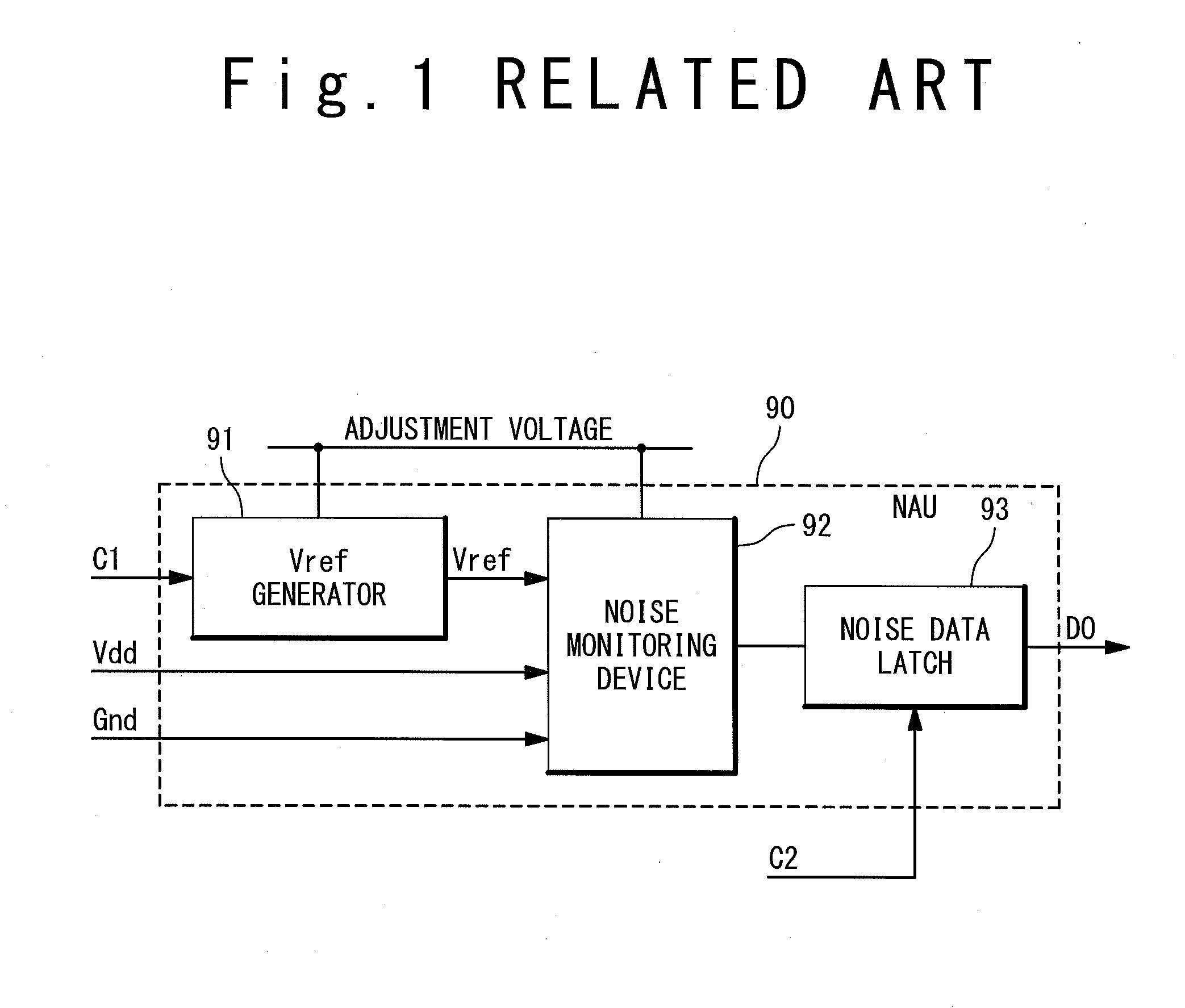
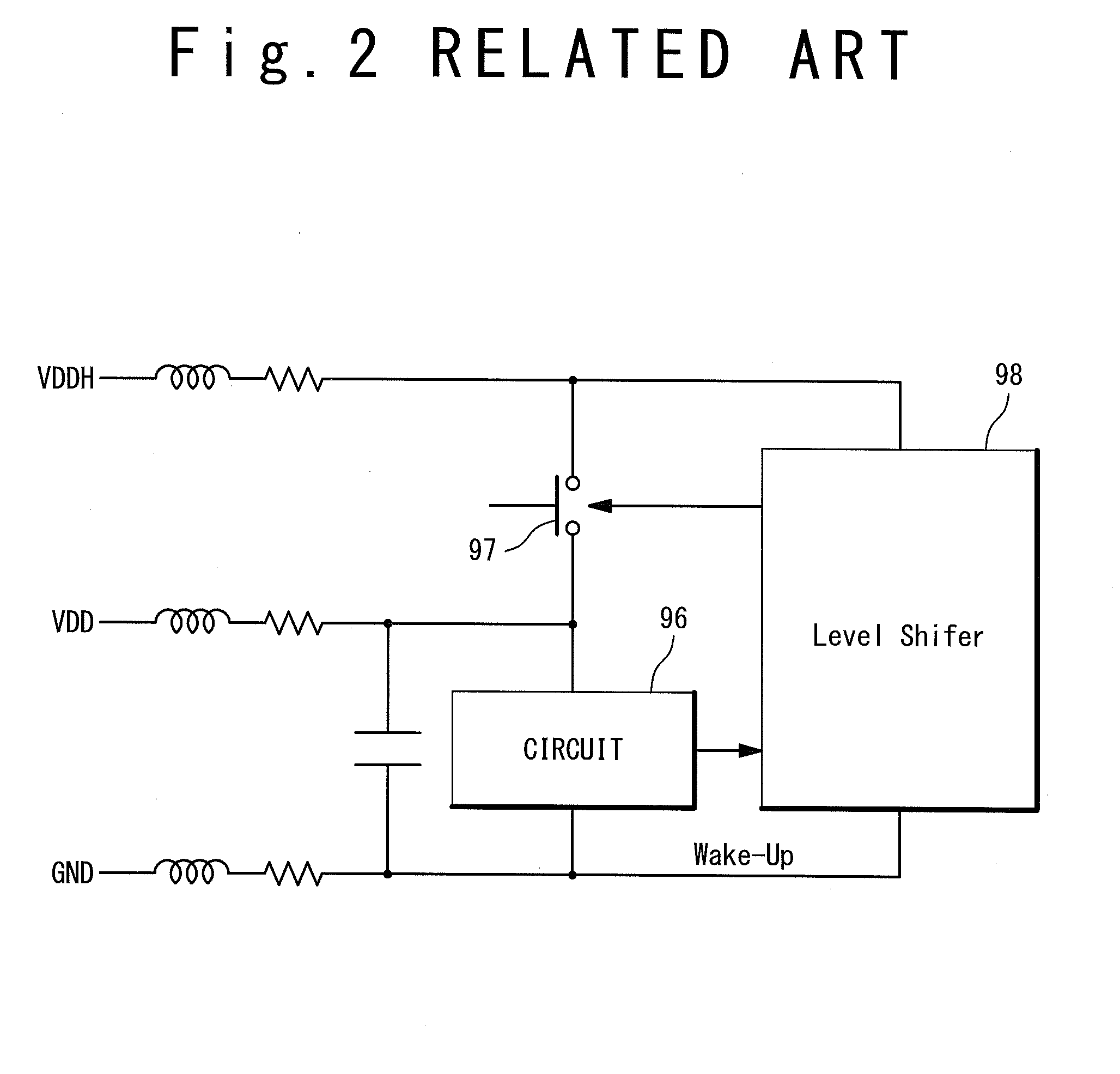
Problems solved by technology
Method used
Image

Examples
first embodiment
The first embodiment will be described below with reference to FIG. 3. As shown in FIG. 3, a semiconductor device according to the first embodiment includes a voltage variation reducing circuit (inverter circuit) 10 in which a voltage GND and a power source voltage VDDH higher than a power source voltage VDD serve as power sources. The voltage variation reducing circuit 10 is connected to a power source line of the voltage VDD at its input and output. The position where the input of the voltage variation reducing circuit 10 is connected to the power source line of the voltage VDD is the position where the power source voltage VDD is monitored. The position where the output of the voltage variation reducing circuit 10 is connected to the power source line of the voltage VDD is the position where a current is supplied to the power source line of the power source voltage VDD, in order to prevent a drop in the voltage VDD. The position where the input of the voltage variation reducing c...
second embodiment
The second embodiment will be described below with reference to FIG. 5. In the second embodiment, the voltage variation reducing circuit 10 reduces a penetration current while suppressing the drop in the voltage VDD.
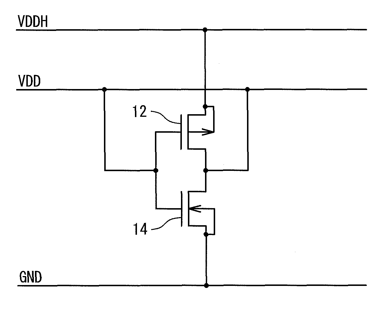
As shown in FIG. 5, the voltage variation reducing circuit 10 according to the second embodiment includes a P-channel MOS transistor 12, an N-channel MOS transistor 14 and a P-channel MOS transistor 16, which are connected in series between the power source line of the voltage VDDH and the power source line of the voltage GND. The P-channel MOS transistor 16 is inserted between the power source line of the voltage GND and the source of the N-channel MOS transistor 14 in the voltage variation reducing circuit 10 described in the first embodiment. The gate of the P-channel MOS transistor 16 and the gates of the P-channel MOS transistor 12 and the N-channel MOS transistor 14 are commonly connected to the voltage VDD.
Thus, the P-channel MOS transistor 12 and the N-channel MO...
third embodiment
The third embodiment will be described below with reference to FIG. 6. In the third embodiment, the action of the voltage variation reducing circuit 10 is controlled.
The voltage variation reducing circuit 10 according to the third embodiment is such that an N-channel MOS transistor 18 is further added to the voltage variation reducing circuit 10 described in the second embodiment. The N-channel MOS transistor 18 is connected in series between the source of the P-channel MOS transistor 12 and the power source line of the power source voltage VDDH. Thus, the drain of the N-channel MOS transistor 18 is connected to the power source line of the voltage VDDH, and the source is connected to the source of the P-channel MOS transistor 12. A control signal CTRL is applied to the gate of the N-channel MOS transistor 18.
When the N-channel MOS transistor 18 is in an on state based on the control signal CTRL, the P-channel MOS transistors 12, 16 and the N-channel MOS transistor 14 are operated a...
PUM
 Abstract
Description
Claims
Application Information