Method for growing germanium epitaxial films

a technology of epitaxial film and germanium, which is applied in the direction of single crystal growth, polycrystalline material growth, chemistry apparatus and processes, etc., can solve the problems of low growth rate of underlying dielectric layer, high defect density, rough germanium film,

Inactive Publication Date: 2011-02-17
BAE SYST INFORMATION & ELECTRONICS SYST INTERGRATION INC
View PDF64 Cites 10 Cited by
  • Summary
  • Abstract
  • Description
  • Claims
  • Application Information

AI Technical Summary

Problems solved by technology

The problem with the first method is that the resultant germanium film is very rough and has a substantially high defect density.
Thus, although the second method overcomes the roughness problem, the resultant germanium film occurs on an underlying silicon layer as well as an underlying dielectric layer.
The growth on the underlying silicon layer is desired but the growth on the underlying dielectric layer is not.

Method used


Image

  • Method for growing germanium epitaxial films
  • Method for growing germanium epitaxial films
  • Method for growing germanium epitaxial films

Examples


Embodiment Construction

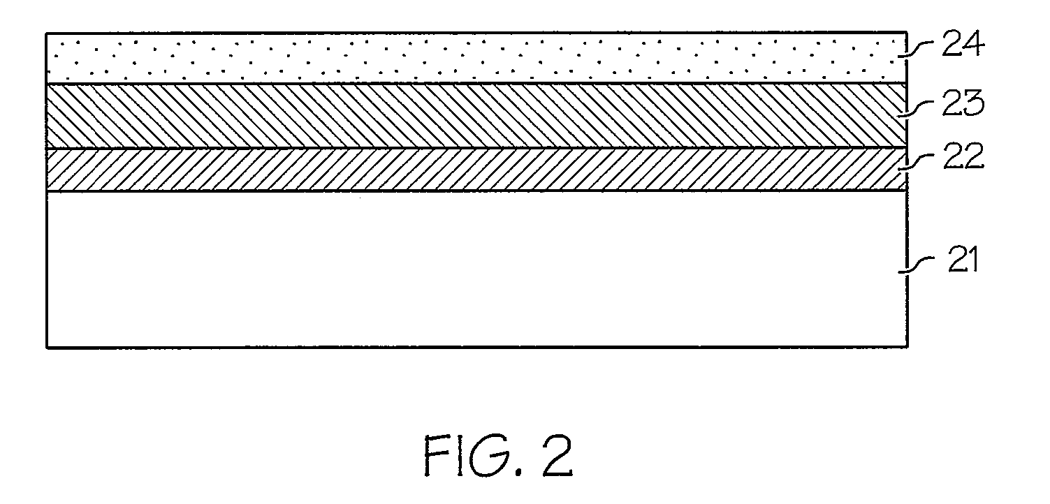
[0012]The desired smooth and highly selective germanium layer is formed using a UHV-CVD system. The formation can be completed by using the following gases: hydrogen, 100% silane (SiH4), 100% germane (GeH4), 1% diborane (B2H6) and 1% phosphine (PH3).

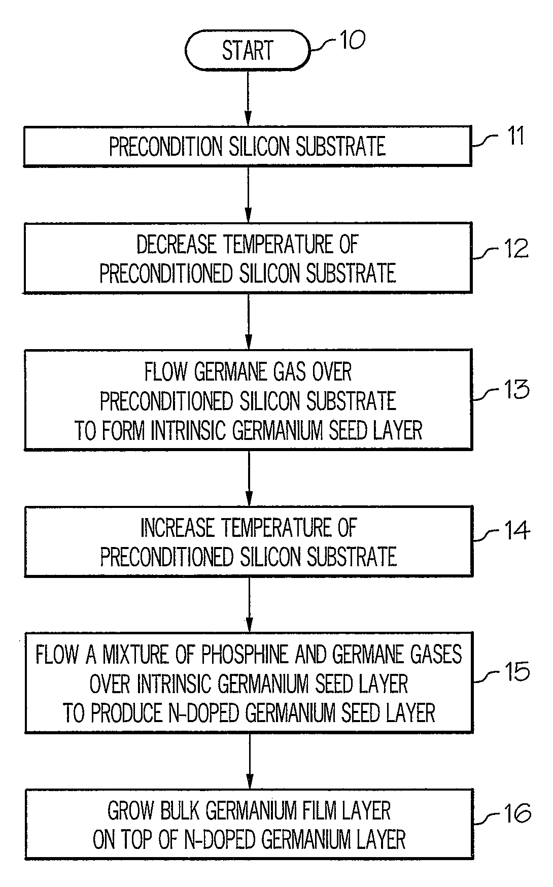
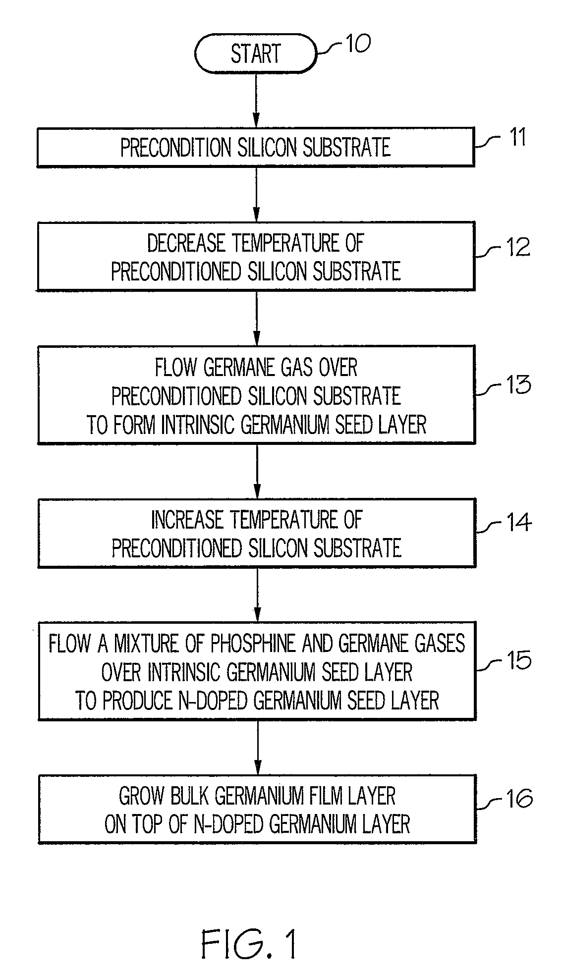
[0013]Referring now to the drawings and in particular to FIG. 1, there is illustrated a high-level process flow diagram of a method for growing germanium epitaxial films, in accordance with a preferred embodiment of the present invention. Starting at block 10, a silicon substrate is preconditioned with hydrogen gas at 750° C. for 60 minutes, as shown in block 11. The pressure of hydrogen is controlled at 3E−4 mBar.

[0014]Next, the temperature is ramped down from 750° C. to 350° C. in 200 minutes in vacuum at 2° C. per minute, as depicted in block 12.

[0015]Germane gas at 1.5E−3 mBar is flowed over the preconditioned silicon substrate for 120 minutes, as shown in block 13. This step initiates the layer-by-layer growth for approximately the ...


PUM

PropertyMeasurementUnit
temperatureaaaaaaaaaa

Abstract

A method for growing germanium epitaxial films is disclosed. Initially, a silicon substrate is preconditioned with hydrogen gas. The temperature of the preconditioned silicon substrate is then decreased, and germane gas is flowed over the preconditioned silicon substrate to form an intrinsic germanium seed layer. Next, a mixture of germane and phosphine gases can be flowed over the intrinsic germanium seed layer to produce an n-doped germanium seed layer. Otherwise, a mixture of diborane and germane gases can be flowed over the intrinsic germanium seed layer to produce a p-doped germanium seed layer. At this point, a bulk germanium layer can be grown on top of the doped germanium seed layer.

Description

BACKGROUND OF THE INVENTION[0001]1. Technical Field[0002]The present invention relates to epitaxial films in general, and in particular to a method for growing germanium epitaxial films on silicon substrates.[0003]2. Description of Related Art[0004]There are two conventional methods for growing single-crystal germanium films on silicon substrates using ultra-high vacuum chemical vapor deposition (UHV-CVD). The first method allows a germanium film to be grown directly on top of a silicon layer, and the second method uses a silicon and silicon germanium buffer layer at the interface.[0005]Since the first method is very selective, a germanium film only grows on a silicon layer and not on any exposed dielectric material. The problem with the first method is that the resultant germanium film is very rough and has a substantially high defect density. Compared with the first method, the second method is not selective at all. Thus, although the second method overcomes the roughness problem,...

Claims


Application Information

Patent Timeline
Patent Type & Authority Applications(United States)
IPC IPC(8): C30B25/02
CPCH01L21/02381H01L21/0245H01L21/02502H01L21/02658H01L21/02579H01L21/0262H01L21/02532H01L21/02645
Inventor CAROTHERS, DANIEL N.HILL, CRAIG M.POMERENE, ANDREW T.S.VU, VU A.
Owner BAE SYST INFORMATION & ELECTRONICS SYST INTERGRATION INC
Why Eureka
Try Eureka