Semiconductor Photodetector Structure and the Fabrication Method Thereof

a technology of semiconductors and photodetectors, applied in the manufacture of final products, basic electric elements, solid-state devices, etc., can solve the problems of reducing the quality of photodetectors, difficult control of the roughness of the germanium layer, and incompatible transmission principles with the basic principle of transmission, so as to achieve better photodetector quality

Active Publication Date: 2011-02-17
UNITED MICROELECTRONICS CORP
View PDF7 Cites 102 Cited by
  • Summary
  • Abstract
  • Description
  • Claims
  • Application Information

AI Technical Summary

Benefits of technology

[0010]The present invention provides a germanium photodetector structure and the method for making the same that can integrate into the traditional MOS manufacturing process and can obtain better photodetector quality.

Problems solved by technology

Conventional copper cables are less and less capable of carrying more and more signals to travel a longer and longer distance due to the physical limitation of electrical resistance and signal delays.
However, such basic principle of transmission is not compatible with the basic principle of transmission by electron current in the current electronic devices to carry and to transmit signals.
However, the germanium layer is non-selectively deposited on the substrate, and should be etched and planarized, making the roughness of the germanium layer hard to control and lowering the photodetecting quality.
However, the direction of the light input and the diode channel is horizontal, which may cause more noise.
And the photodetector is fabricated on a SOI substrate, which increases the manufacturing cost.

Method used


Image

  • Semiconductor Photodetector Structure and the Fabrication Method Thereof
  • Semiconductor Photodetector Structure and the Fabrication Method Thereof
  • Semiconductor Photodetector Structure and the Fabrication Method Thereof

Examples


Embodiment Construction

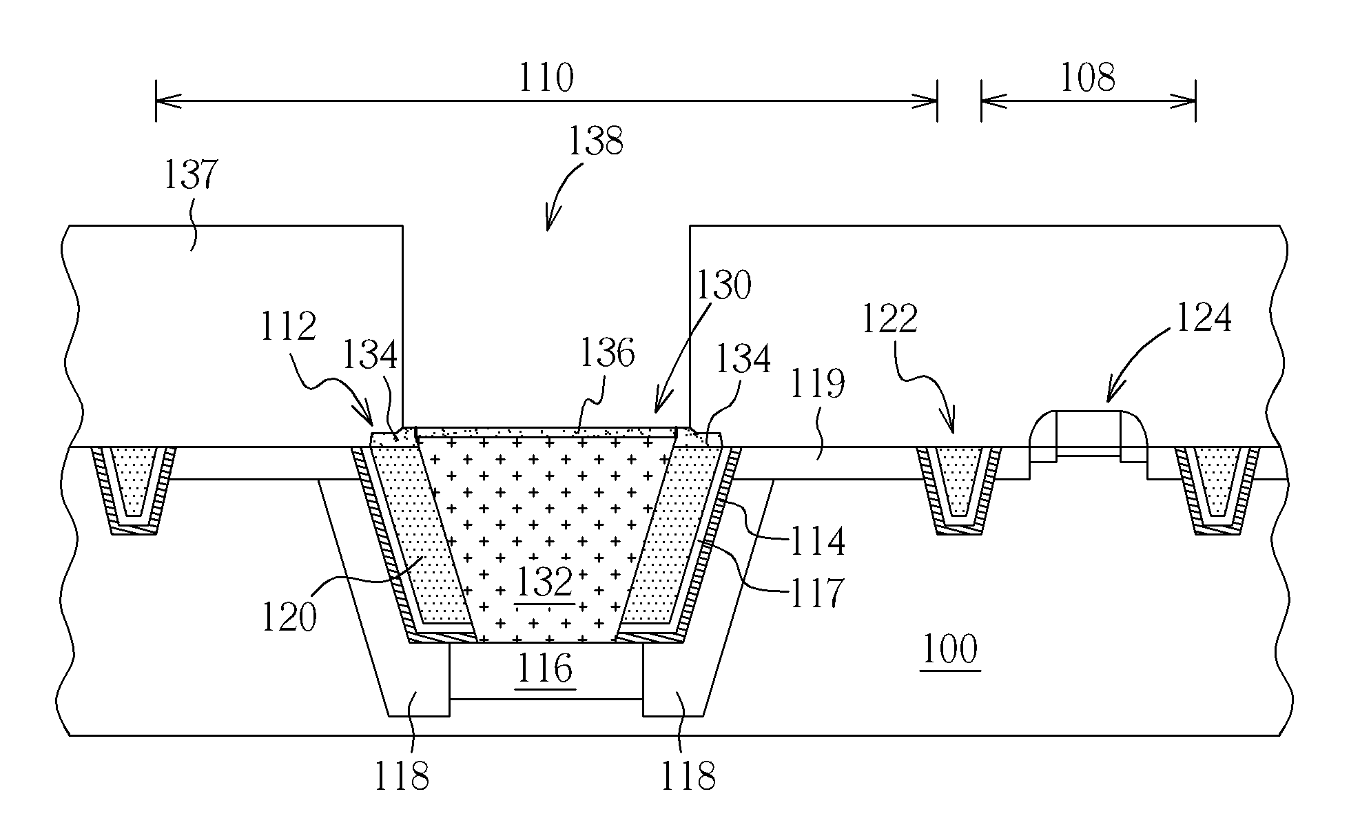
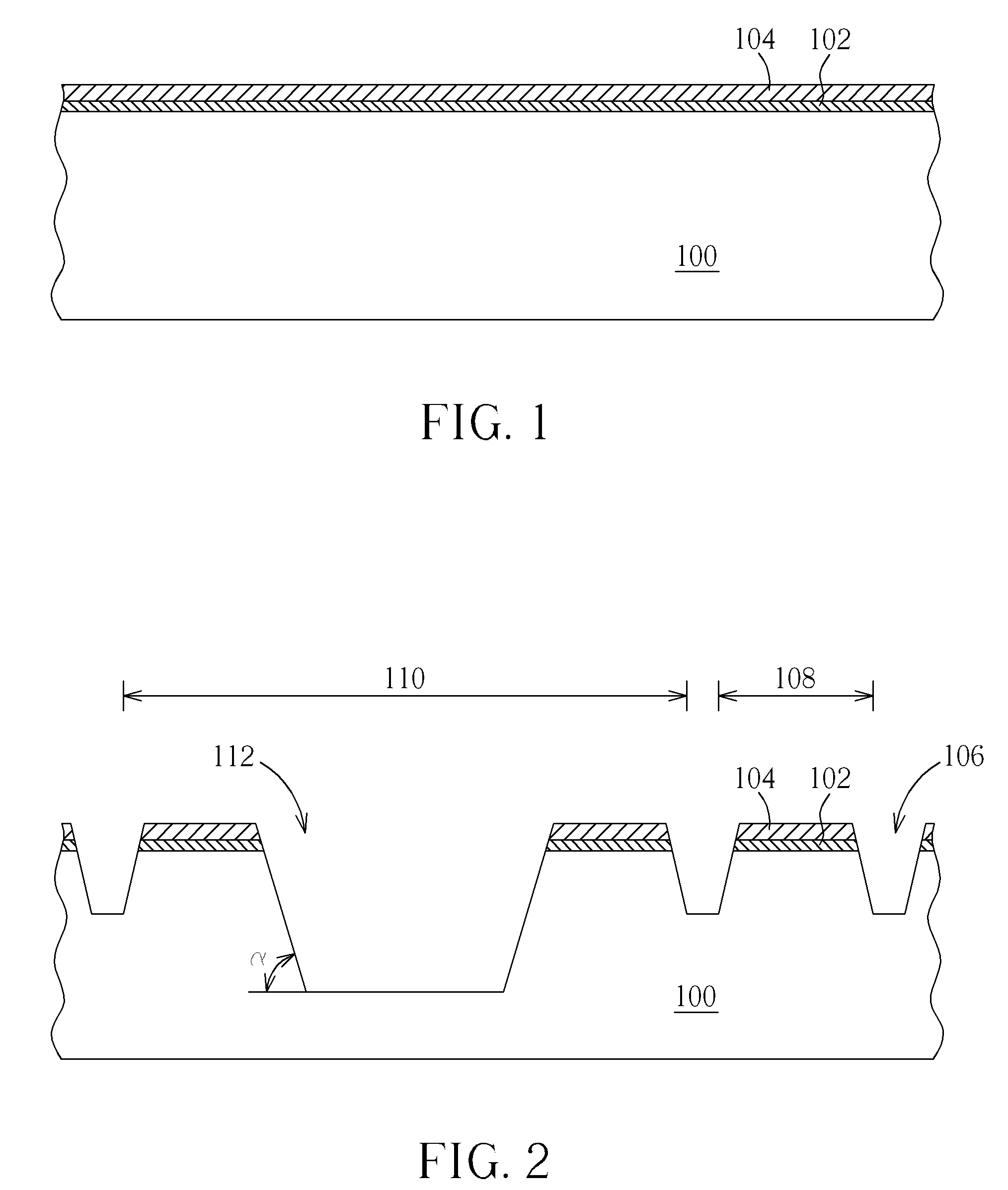
[0018]Please refer to FIG. 1 to FIG. 11, illustrating the schematic diagrams of the method of fabricating the semiconductor photodetector structure in the present invention. Please refer to FIG. 1. First, a substrate100 is provided. Then, an oxide layer 102 and a nitride layer 104 are deposited on the substrate 100. The substrate 100 may include general semiconductor material, such as a silicon substrate.

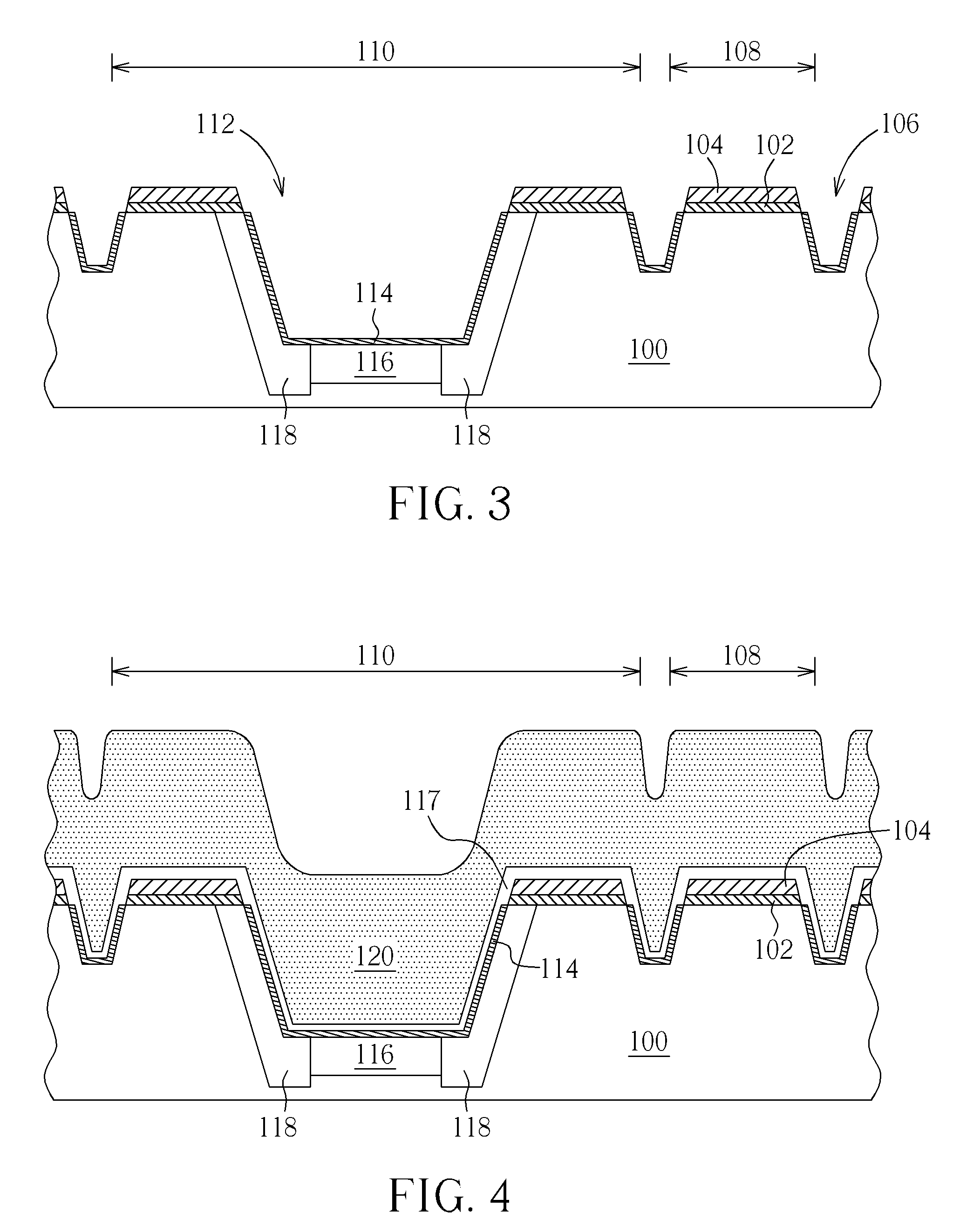
[0019]Then an active region 108 and a photodetecting region 110 on the substrate 100 are defined. In the follow-up steps, an active component such as a MOS will be formed in the active region 108 and a photodetector will be formed in the photodetecting region 110. Next, a patterning process is provided to form a plurality of shallow trenches 106 around the active region 108. Generally, the shallow trench has a depth about 300-400 nm. Then, another patterning process is performed to form a deep trench 112 in the photodetecting region 110 of the substrate 100. The deep trench 112 has ...


PUM


Abstract

A semiconductor photodetector structure is provided. The structure includes a substrate, a photodetecting element and a semiconductor layer disposed on the photodetecting element. The substrate includes a first semiconductor material and includes a deep trench. The surface of the deep trench includes a first type dopant. The photodetecting element is disposed in the deep trench. The photodetecting element includes a second semiconductor material. The semiconductor layer includes a second type dopant.

Description

BACKGROUND OF THE INVENTION[0001]1. Field of the Invention[0002]The invention relates to a semiconductor photodetector structure, especially to a photodetector structure that includes germanium semiconductor material.[0003]2. Description of the Prior Art[0004]Conventional copper cables are less and less capable of carrying more and more signals to travel a longer and longer distance due to the physical limitation of electrical resistance and signal delays. Naturally, optical fibers meet the demand of carrying very large information to travel a very long distance so they replace the conventional copper cables to be the medium of long distance carrier of information because one single optical fiber allows multiple beams of light of different wavelengths, each carrying different information to travel at the speed of light without mutual interference and without attenuating too much after traveling an extreme long distance.[0005]Light of different wavelengths in the form of pulse signal...

Claims


Application Information

Patent Timeline
Patent Type & Authority Applications(United States)
IPC IPC(8): H01L31/0232H01L31/18H01L31/08
CPCH01L27/1461H01L31/035281Y02E10/547H01L31/1804H01L31/1808H01L31/105Y02P70/50
Inventor SU, TZUNG-ILAN, BANG-CHIANGSU, CHAO-ANWU, HUI-MINWANG, MING-IHUANG, CHIEN-HSINTAN, TZUNG-HANCHEN, MINLIN, MENG-JIASU, WEN-YU
Owner UNITED MICROELECTRONICS CORP
Why Eureka
Try Eureka