Solid-state image sensing element and image sensing system

a sensing element and image technology, applied in the field of solid-state image sensing element and image sensing system, can solve the problems of large the influence of circuit noise is relatively serious, and the noise in the wideband circuit is large, so as to achieve high a/d conversion speed and reduce noise

Active Publication Date: 2011-02-17
CANON KK
View PDF24 Cites 82 Cited by
  • Summary
  • Abstract
  • Description
  • Claims
  • Application Information

AI Technical Summary

Benefits of technology

[0011]According to the solid-state image sensing element and image sensing system of the prese

Problems solved by technology

In general, a wideband circuit suffers large noise.
This is because such circuits undesirably transmit noise components distributed over a broad frequency band.
In this case, even if the A/D conversion resolution is raised any further, circuit noise becomes dominant, and lower bits include only noise components.
In pa

Method used


Image

  • Solid-state image sensing element and image sensing system
  • Solid-state image sensing element and image sensing system
  • Solid-state image sensing element and image sensing system

Examples


first embodiment

Effect of First Embodiment

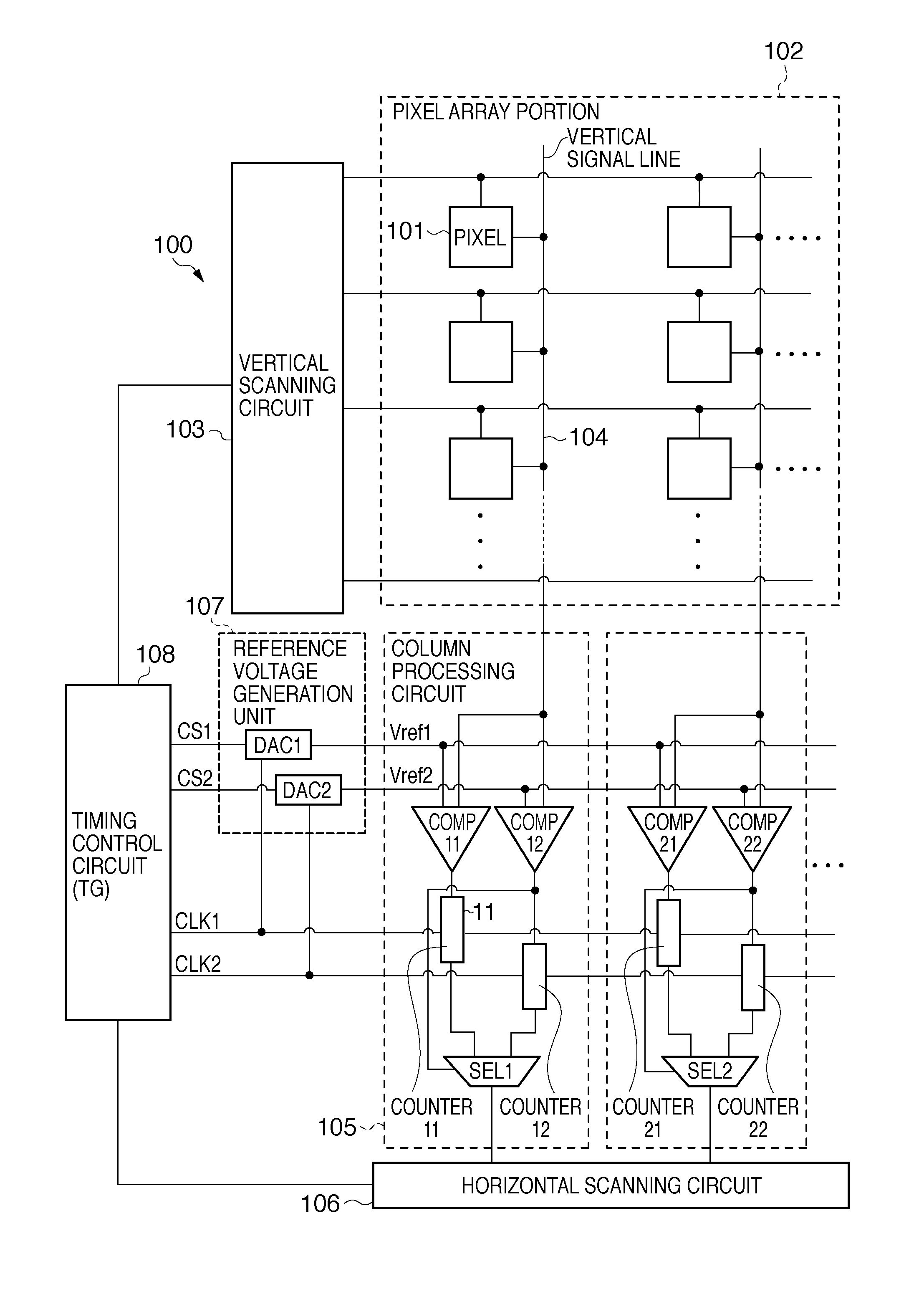
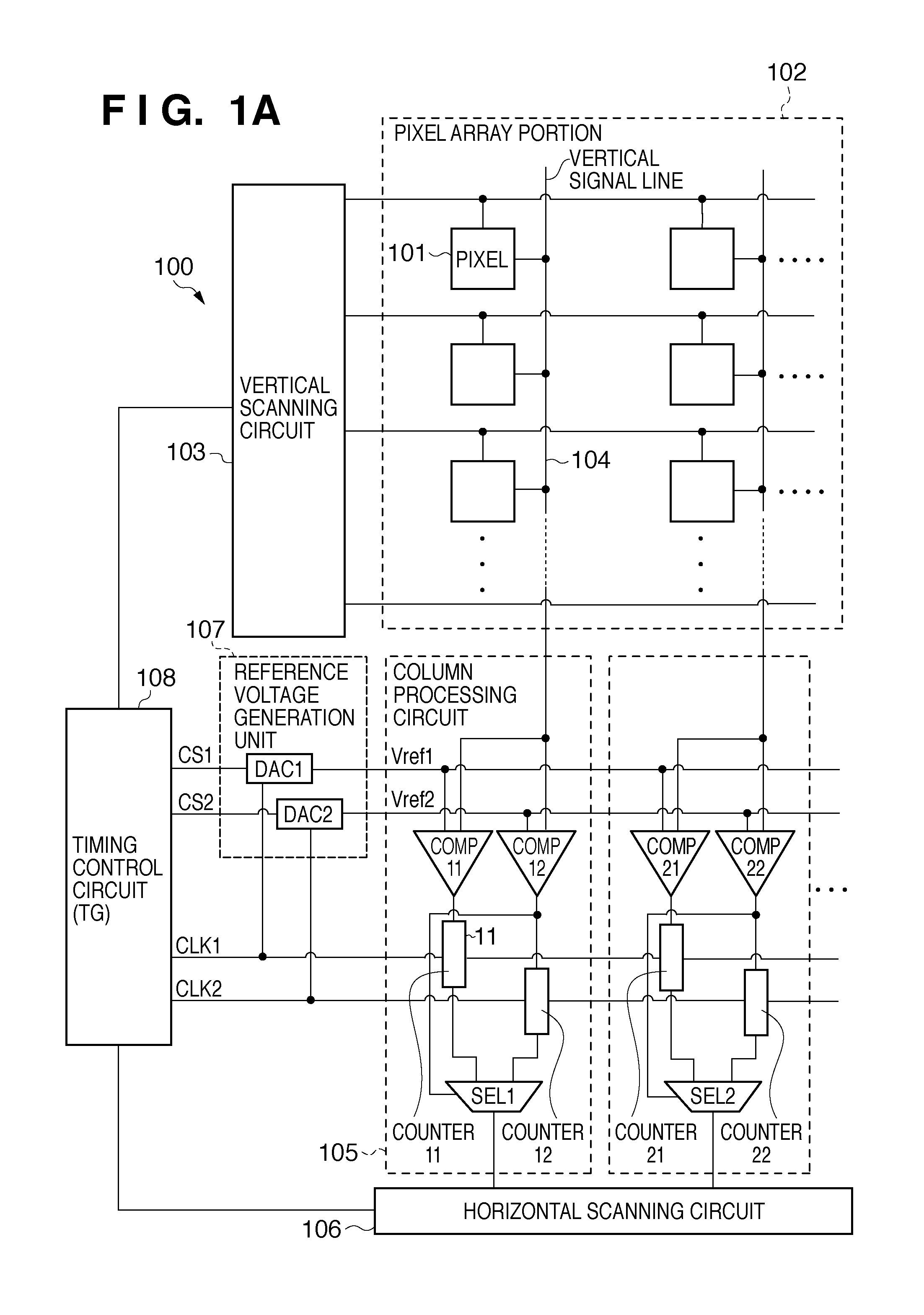
[0038]As described above, the first embodiment adopts the arrangement in which the solid-state image sensing element 100 includes the plurality of comparison circuits having different frequency band characteristics in the comparison unit used in the A / D conversion, and these comparison circuits are selectively applied according to the signal level of the pixel signal Vsig. According to this arrangement, when a signal level which is practically influenced by circuit noise is low, the A / D conversion with less circuit noise is executed; when the signal level is high, the A / D conversion including high-speed signal comparison is executed. Therefore, the solid-state image sensing element which can output a high-precision digital signal at high speed can be provided.

Second Embodiment

Arrangement Example of Solid-State Image Sensing Element of Second Embodiment

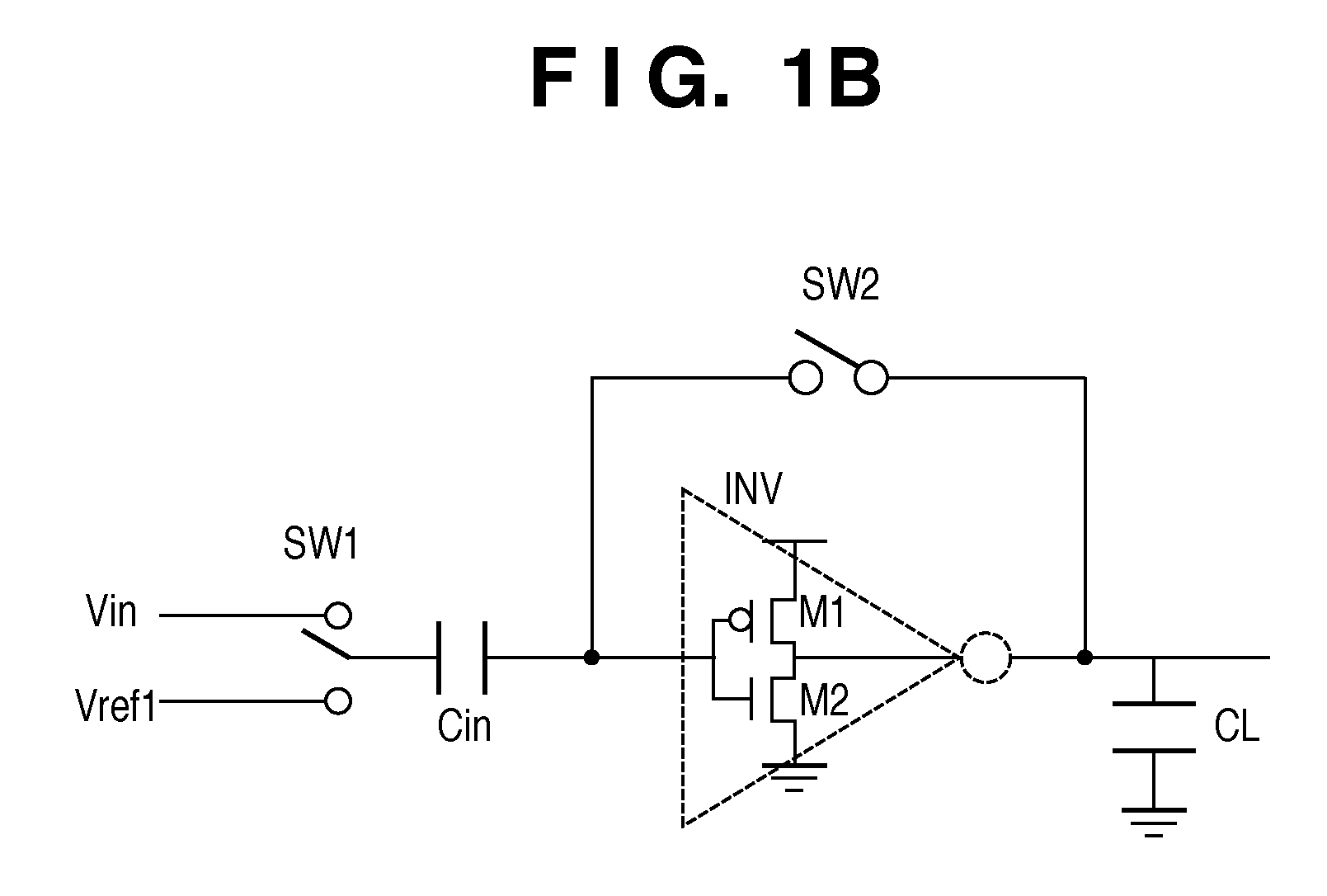
[0039]FIG. 4 is a block diagram showing an example of the arrangement of a solid-state image sensing elemen...

second embodiment

Effect of Second Embodiment

[0047]As described above, according to the second embodiment, the solid-state image sensing element 500 adopts the arrangement in which the frequency band characteristic of the comparison circuit COMPx1 used in A / D conversion, the reference voltages, and the operations of other peripheral circuits can be easily switched based on the output level of the pixel signal Vsig. According to this arrangement, when a signal level which is practically influenced by circuit noise is low, the A / D conversion with less circuit noise is executed; when the signal level is large to some extent, the A / D conversion including high-speed signal comparison is executed. Therefore, the solid-state image sensing element which can output a high-precision digital signal at high speed can be provided.

Arrangement Example of Image Sensing System of This Embodiment

[0048]The solid-state image sensing elements of the first and second embodiments can be used as an image sensing element of ...


PUM


Abstract

In a solid-state image sensing element which includes a pixel array portion in which a plurality of pixels each including a photoelectric converter are arranged two-dimensionally, and readout circuits which read out analog pixel signals from the pixel array portion by column, and in which each of the readout circuits includes an A/D conversion circuit which converts the analog pixel signal from the pixel array portion into a digital pixel signal, and the A/D conversion circuit performs A/D conversion by comparing, by a comparison unit, a signal level of the analog pixel signal from the pixel array portion with a temporally changing reference level, a frequency band characteristic of the comparison unit is switched in accordance with the signal level of the analog pixel signal from the pixel array portion.

Description

BACKGROUND OF THE INVENTION[0001]1. Field of the Invention[0002]The present invention relates to a solid-state image sensing element and image sensing system and, more particularly, to a solid-state image sensing element which includes column A / D conversion circuits that perform analog-to-digital conversion of pixel signals from two-dimensionally arranged pixels by column, and an image sensing system using the solid-state image sensing element.[0003]2. Description of the Related Art[0004]In recent years, X-Y addressing type solid-state image sensing elements, such as a CMOS sensors, have emerged which includes circuits that perform analog-to-digital conversion (to be referred to as A / D conversion hereinafter) by column. Such solid-state image sensing element converts analog signals from pixels into digital signals in an early stage of a signal path, thereby preventing noise from superimposing on signals, and improving an S / N. Also, A / D conversion processing can be executed in a colu...

Claims


Application Information

Patent Timeline
IPC IPC(8): H04N5/335H04N5/228
CPCH04N5/357H03M1/188H04N5/3742H03M1/123H03M1/56H04N5/378H04N25/60H04N25/767H04N25/75H04N25/78
Inventor OTA, KEISUKE
Owner CANON KK
Why Eureka
Try Eureka