

Semiconductor device and method for manufacturing the same
- Summary
- Abstract
- Description
- Claims
- Application Information
AI Technical Summary
Benefits of technology
Problems solved by technology
Method used
Image

Examples
example 1
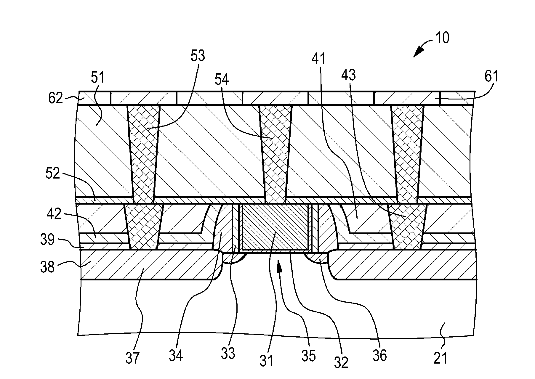
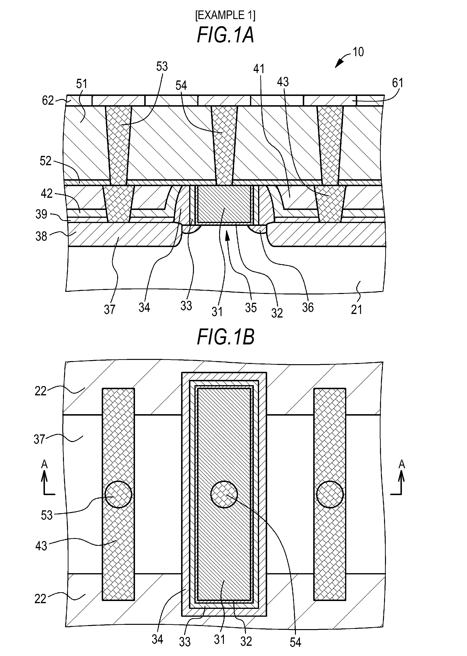
[0098]Example 1 concerns the semiconductor device and the semiconductor device manufacturing method according to First Embodiment of the present invention. Example 1 employs the gate electrode forming method of First Embodiment. FIG. 1A is a schematic partial end view of a semiconductor device of Example 1 along the gate length. FIG. 1B schematically illustrates the layout of each constituting element of the semiconductor device of Example 1 as viewed from above. Note that the schematic partial end view shown in FIG. 1A is taken at A-A indicated by arrows in FIG. 1B.
[0099]A semiconductor device 10 of Example 1 includes:
[0100](A) source / drain regions 37 and a channel forming region 35 formed in a substrate (specifically, a silicon semiconductor substrate 21);
[0101](B) a gate electrode 31 provided above the channel forming region 35 via a gate insulating film 32;
[0102](C) a first interlayer insulating layer 41 formed on the source / drain regions 37;
[0103](D) first contact portions 43 f...
example 2
[0133]Example 2 is a variation of the semiconductor device manufacturing method of Example 1. Example 2 employs the gate electrode forming method of Second Embodiment. Specifically, a gate electrode 131 is formed on a substrate (silicon semiconductor substrate), and after forming source / drain regions 37 and a channel forming region 35 in the substrate, a first interlayer insulating layer 41 whose top face lies within the same plane as the top face of the gate electrode 131 is formed on the source / drain regions 37. Note that Example 2 differs from Example 1 in that the gate insulating film 132 does not extend between the first interlayer insulating layer 41 and the gate electrode 131.
[0134]The semiconductor device manufacturing method of Example 2 is described below with reference to the schematic partial end views of the substrate and other elements illustrated in FIGS. 8A, 8B, and 8C, FIGS. 9A, 9B, and 9C, FIGS. 10A, 10B, and 10C, FIGS. 11A, 11B, and 11C, and FIGS. 12A and 12B.
[Ste...
example 3
[0146]Example 3 concerns the semiconductor device and the semiconductor device manufacturing method according to Second Embodiment of the present invention. Example 3 employs the gate electrode forming method of First Embodiment. The semiconductor device of Example 3 is a CMOS-type semiconductor device of a dual gate structure, and includes an n-channel semiconductor device and a p-channel semiconductor device. The structures and configurations of the n-channel semiconductor device and the p-channel semiconductor device are the same as those of the semiconductor device 10 described in Example 1, and detailed descriptions thereof are omitted here.
[0147]FIG. 13 schematically illustrate the layout of each constituting element of the semiconductor device of Example 3 as viewed from above. As illustrated in the figure, an n-channel semiconductor device 10N and a p-channel semiconductor device 10P have first contact portions 43N and 43P, respectively, that are groove-shaped and join toget...
PUM
 Abstract
Description
Claims
Application Information