Three-Dimensional Silicon Interposer for Low Voltage Low Power Systems

a silicon interposer and low power technology, applied in the field of interconnect technology, can solve the problems of increasing errors, chip stacks or across multiple chips not receiving the proper voltage, and the scaling requirements of today's electronic devices, and achieve the effect of low voltage and low power operations

Active Publication Date: 2011-02-24
IBM CORP
View PDF16 Cites 130 Cited by
  • Summary
  • Abstract
  • Description
  • Claims
  • Application Information

AI Technical Summary

Benefits of technology

[0010]The present invention provides scalable silicon (Si) interposer configurations that support low voltage, low power operations. In one aspect of the invention, a Si interposer is provided. The Si interposer comprises a plurality of through-silicon vias (TSVs) within a first plane of the interposer, wherein the TSVs are adapted to serve as power, ground and signal interconnections throughout the first plane such that the TSVs that serve as the power and ground interconnections are greater in at least one of number and size than the TSVs that serve as the signal interconnections so as to sup

Problems solved by technology

The scaling requirements of today's electronic devices present a challenge with regard to providing the proper power, ground, signal and/or various other connections to each component within a device.
A combination of aggressive scaling and low power levels can undesirably lead to an increased amount of errors.
Thus, depending on the severity of the voltage droop, transistors or circuits in a chip, a chip stack or across multiple chips may not receive the proper voltage and not operate properly or operate with errors.
This area array input/output (I/O) distancing practice along with typically limited X-Y power and ground cross-sectional size for power grids on a chip, as well as more simultaneous switc

Method used


Image

  • Three-Dimensional Silicon Interposer for Low Voltage Low Power Systems
  • Three-Dimensional Silicon Interposer for Low Voltage Low Power Systems
  • Three-Dimensional Silicon Interposer for Low Voltage Low Power Systems

Examples


Embodiment Construction

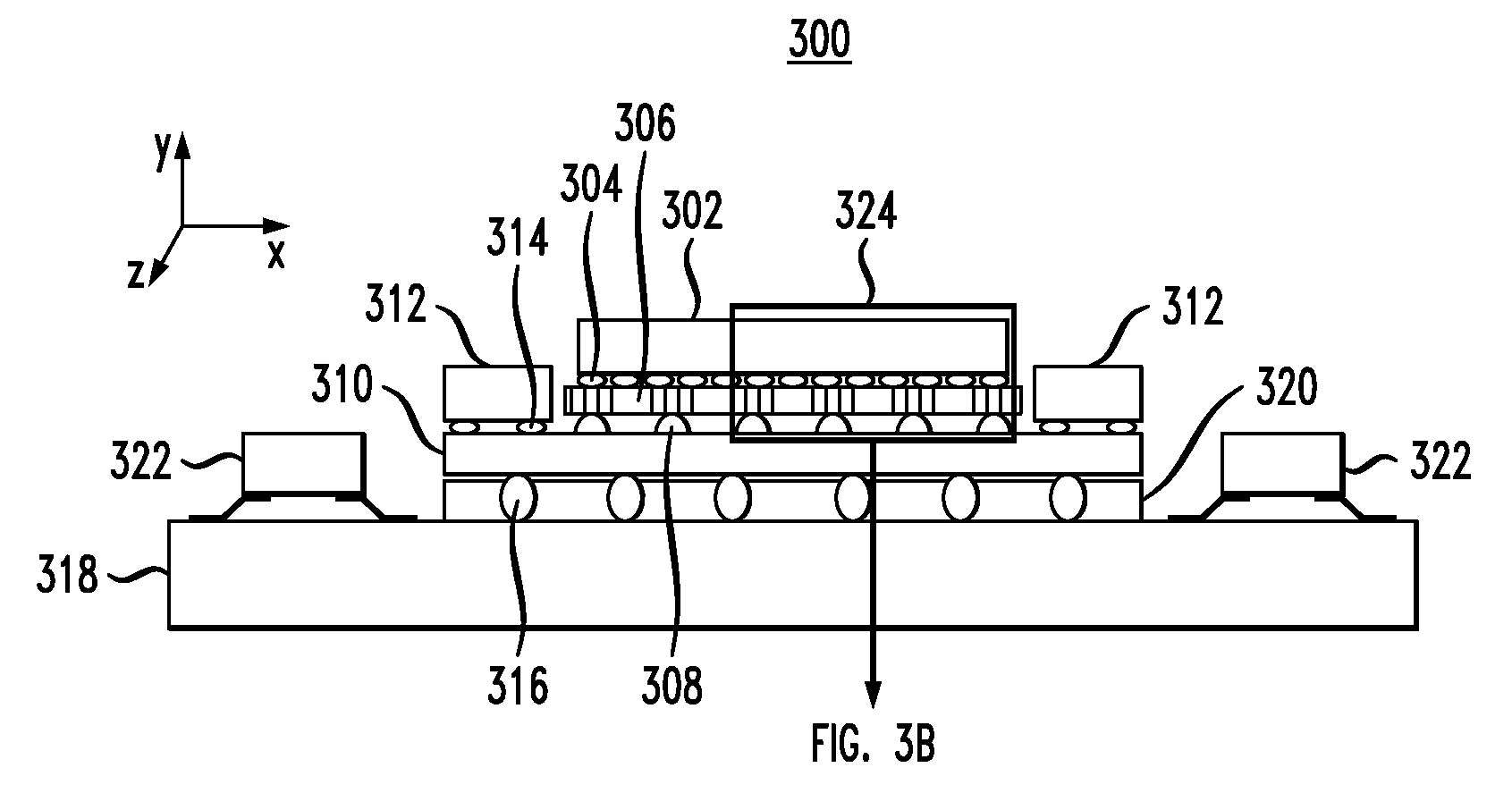
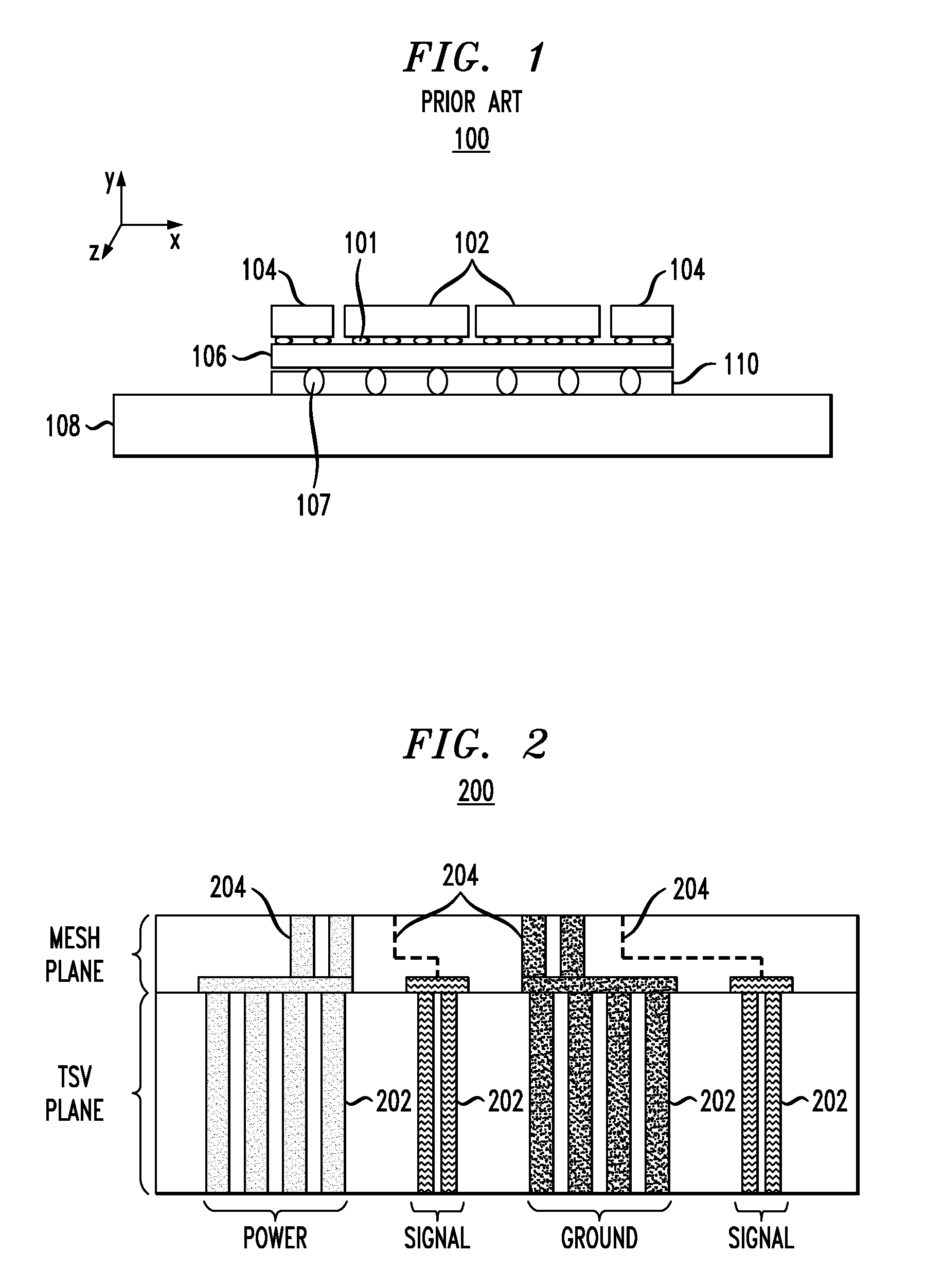
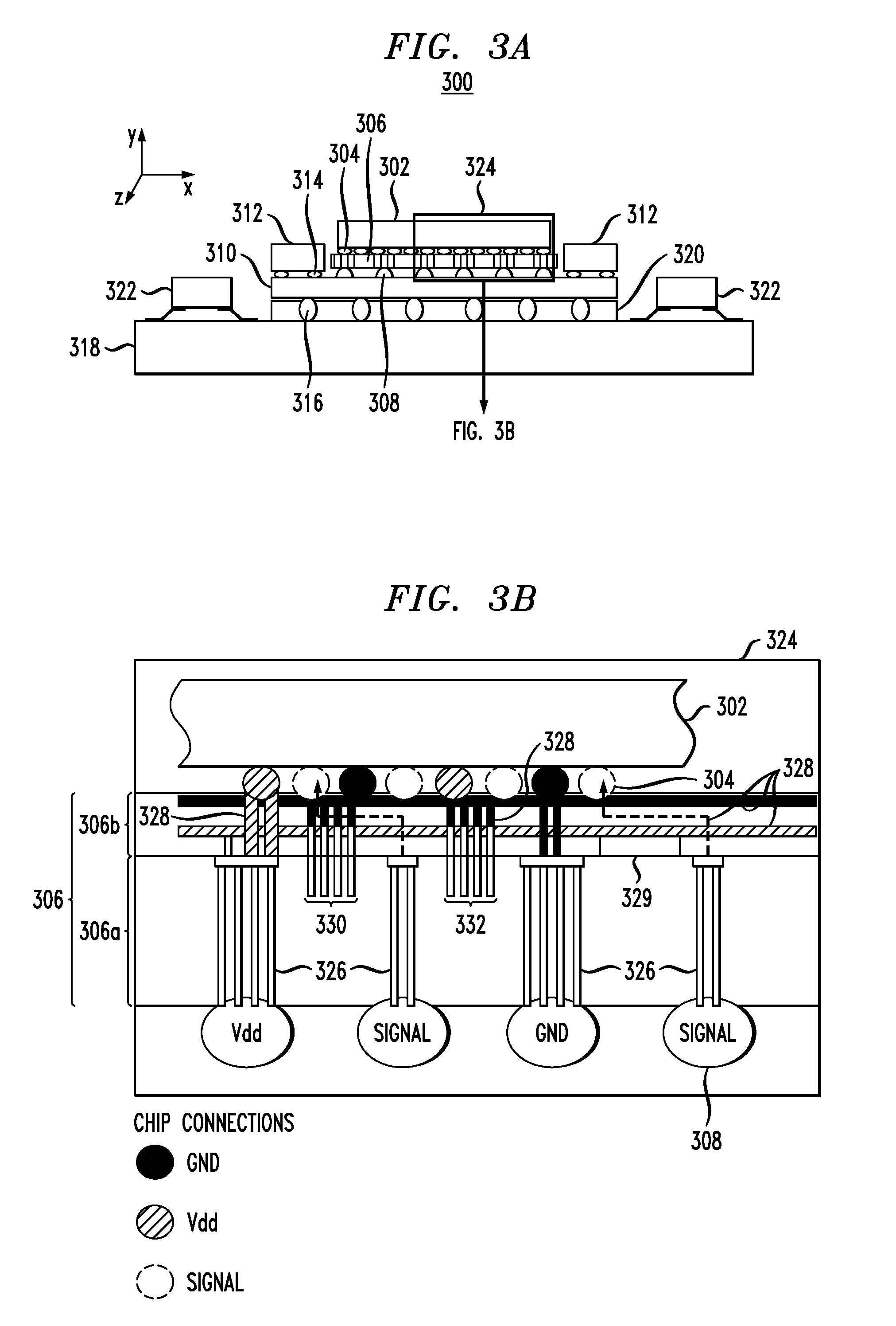
[0024]FIG. 2 is a cross-sectional diagram illustrating exemplary silicon (Si) interposer 200. An interposer structure is sometimes also referred to in the semiconductor arts as a platform and / or as a carrier. Often these terms are used interchangeably. For consistency, the term “interposer” is used herein throughout. Si interposer 200 includes through-silicon vias (TSVs) 202 within a first plane thereof (this first plane of Si interposer 200 is also referred to herein as a TSV plane). TSVs 202 serve as power, ground and signal interconnections throughout the TSV plane. One advantage of the present teachings is that Si interposer 200 supports uniform power distribution therethrough even during low voltage operations. According to one exemplary embodiment, in order to support uniform power distribution through Si interposer 200 during low voltage operations (for example, during low voltage operations of less than 500 millivolts (mV), e.g., during low voltage operations of less than 30...


PUM


Abstract

Scalable silicon (Si) interposer configurations that support low voltage, low power operations are provided. In one aspect, a Si interposer is provided which includes a plurality of through-silicon vias (TSVs) within a first plane thereof adapted to serve as power, ground and signal interconnections throughout the first plane such that the TSVs that serve as the power and ground interconnections are greater in number and/or size than the TSVs that serve as the signal interconnections; and a plurality of lines within a second plane of the interposer in contact with one or more of the TSVs in the first plane, the second plane being adjacent to the first plane, adapted to serve as power, ground and signal interconnections throughout the second plane such that the lines that serve as the power and the ground interconnections are greater in number and/or size than the lines that serve as the signal interconnections.

Description

STATEMENT OF GOVERNMENT RIGHTS[0001]This invention was made with Government support under Contract number H98230-07-C-0409 awarded by National Security Agency. The Government has certain rights in this invention.FIELD OF THE INVENTION[0002]The present invention relates to interconnect technology, and more particularly, to scalable silicon (Si) interposer configurations that support low voltage, low power operations.BACKGROUND OF THE INVENTION[0003]The scaling requirements of today's electronic devices present a challenge with regard to providing the proper power, ground, signal and / or various other connections to each component within a device. For example, chips with area array interconnections having a pitch of 200 micrometers (μm), or less, are now common. Interconnect structures having a multitude of line paths therethrough are generally used to connect the chips to a printed wire board. Thus, the lines must also be scalable to accommodate such closely-spaced connections on the ...

Claims


Application Information

Patent Timeline
IPC IPC(8): H01L23/535H01L23/48H01L21/768
CPCH01L21/486H01L2224/16235H01L23/481H01L23/49827H01L23/50H01L24/17H01L25/0657H01L25/16H01L25/18H01L2225/06527H01L2225/06572H01L2924/04941H01L2924/15311H01L2924/19105H01L2924/3025H01L2224/16145H01L2224/16225H01L23/147
Inventor KNICKERBOCKER, JOHN U.
Owner IBM CORP
Why Eureka
Try Eureka