
Spectrally compensating a light sensor

a light sensor and spectral compensation technology, applied in the direction of optical radiation measurement, instruments, spectrometry/spectrophotometry/monochromators, etc., can solve the problem of reducing the proportion of incident light that can be detected by the sensor by using colour filters, and the sensitivity is generally limited by surface reflection, so as to achieve a relatively simple correction algorithm

Inactive Publication Date: 2011-02-24
SHARP KK
View PDF12 Cites 14 Cited by
  • Summary
  • Abstract
  • Description
  • Claims
  • Application Information

AI Technical Summary

Benefits of technology

[0062]A third advantage of the invention is that the correction algorithm is relatively simple, merely requiring a subtraction or the computation of a ratio N and some simple function thereof. Such a method is well suited to an AMLCD where the demands on module size and power consumption make it preferable for the digital processing power to be as small as possible.
[0063]At least one of the first photodetector and the second photodetector may have spectral characteristics that vary over its active area.
[0064]At least a first part of the active area of the first photodetector may be sensitive in the first wavelength range and at least a second, different part of the active area of the first photodetector may be sensitive in a wavelength range different from the first wavelength range
[0065]A second aspect of the present invention provides a light sensor comprising: a first photodetector sensitive in a first wavelength range; a second photodetector sensitive in a second wavelength range different from the first wavelength range and a third photodetector sensitive in a third wavelength range different from the first wavelength range and the second wavelength range; a storage means for storing a plurality of pre-determined corrections for compensating the output of the first photodetector for a difference between a spectral response characteristic of the first photodetector and a reference spectral response characteristic; and a processor for selecting one of the stored corrections, using a ratio of an output of the second photodetector to an output of the first photodetector and a ratio of an output of the third photodetector to the output of the first photodetector; wherein the first wavelength range substantially corresponds to a wavelength range of interest; wherein the second wavelength range is a part of the wavelength range of interest; and wherein the third wavelength range is another part of the wavelength range of interest.
[0066]The wavelength range of interest may be a visible wavelength range. It may correspond substantially to the visible spectrum—that is, cover the wavelength range from approximately 400 nm to approximately 700 nm.

Problems solved by technology

At short wavelengths, where the semiconductor material is a good absorber of the incident light, the sensitivity is generally limited by surface reflections and by absorption of light in non photosensitive parts of the device (e.g. depending on exact the construction of the device these could be passivation layers, gate insulator layers, etc).
There are, however, two significant disadvantages associated with this method.
Firstly the spectral matching to the eye (for example as quantified by the parameter f1), whilst being improved upon compared to the uncorrected sensor, may still be quite poor in comparison with a bulk photosensor device.
A second disadvantage is that the use of colour filters significantly reduces the proportion of the incident light that can be detected by the sensor (since much of the light is absorbed or reflected by the colour filter).
This is a significant disadvantage since in general it is difficult to design a thin film photodetector capable of measuring the low levels of ambient light required by an ALS.
A disadvantage is the extra complexity introduced.
This method would not therefore be at all well suited to a thin film process where just a single thin film layer of semiconductor material is deposited.
A disadvantage of this method is that a large number of output pixels of data are required to obtain statistical information.
EP1107222 does not however address differences between the spectral characteristic of a silicon photodiode and a desired spectral characteristic.

Method used


Image

  • Spectrally compensating a light sensor
  • Spectrally compensating a light sensor
  • Spectrally compensating a light sensor

Examples


first embodiment

[0105]The spectral compensation processing circuitry 138 acts in use as a processor for processing the outputs of the two light sensors to give a spectrally-corrected measure of light intensity. In a first embodiment the processing circuitry evaluates (step 202) the value of parameter X, the quantity W−μ×col1. The circuit 138 may do this through a simple computer program operated by a digital processor.

[0106]In this embodiment spectral compensation is performed by the following method, shown in FIG. 10:[0107]Measure the outputs col1 and W separately from each photosensor 52, 60;[0108]Calculate X=W−μ×col1 (step 202).

[0109]The quantity X is then representative of the spectrally corrected light level. The value of the scaling constant μ will be dependent on the spectral response characteristic of the sensor and the colour filter. A possible method for calculating an appropriate value of μ is as follows, shown FIG. 11:[0110]For a sensor element having quantum efficiency function Q(λ) an...

second embodiment

[0125]The second embodiment has a light sensor comprising the following elements:[0126]A plurality of colour photodetection elements 60, 62 . . . 82 for example photodiodes, each having a colour filter of different spectral characteristics located between its photosensitive region and the direction of the incoming illumination to be detected;[0127]A white photodetection element 52, for example a photodiode having no colour filter;[0128]A means for detecting the light levels as measured by the white and colour photodetection elements, W and col1, col2 . . . colN respectively.

[0129]The spectral compensation circuit 138 consists of the following:[0130]A means 206 for using the outputs col1, col2 . . . colN of the colour photodetectors to correct the output W of the white photodetector, for example by evaluating the quantity

X=W-∑i(μi×coli);

this may be done, for example, by a simple computer program operating in Digital Signal Processing.

[0131]The system operates so as to:[0132]Measure t...

third embodiment

[0139]A third embodiment is illustrated in FIG. 14. In this embodiment a light sensor comprises the following elements:[0140]A colour photodetection element 60 which has a colour filter, for example as the blue colour filter 36 shown FIG. 3, located between its photosensitive region and the direction of the incoming illumination to be detected.[0141]A white photodetection element 52 having no colour filter.[0142]A means for detecting the light levels as measured by the white and colour photodetection elements, W and col1 respectively.

[0143]In this embodiment the spectral compensation processing circuit 138 consists of:[0144]A means 54 for evaluating the value of the parameter N, the ratio col1 / W[0145]A means 56 for calculating the value of the function g(N) for the measured value of the parameter N, for example according to a simple computer program, where g is some simple function of the variable N, for example a polynomial.[0146]A means 58 for calculating the value (for the measur...


PUM


Abstract

A light sensor comprises a first photodetector (52) sensitive in a first wavelength range; a second photodetector (60) sensitive in a second wavelength range different from the first wavelength range; and a processor for determining, using the output of the second photodetector, a correction to the output of the first photodetector for compensating the output of the first photodetector for a difference between the spectral response characteristic of the first photodetector and a reference spectral response characteristic. The processor is adapted to apply the correction to the output of the first photodetector. For example, the first photodetector (52) may be sensitive over the entire visible wavelength range and the second photodetector (60) may be sensitive in a blue wavelength range—this allows the output of the first photodetector to be corrected for an increased sensitivity in the blue wavelength range compared to the reference spectral response characteristic. The light sensor may be used in an Ambient Light Sensing (ALS) system, for example in the ALS of a display.

Description

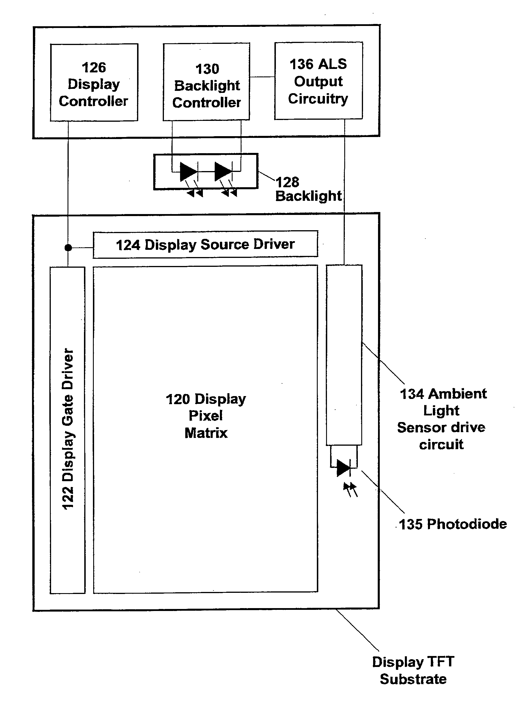
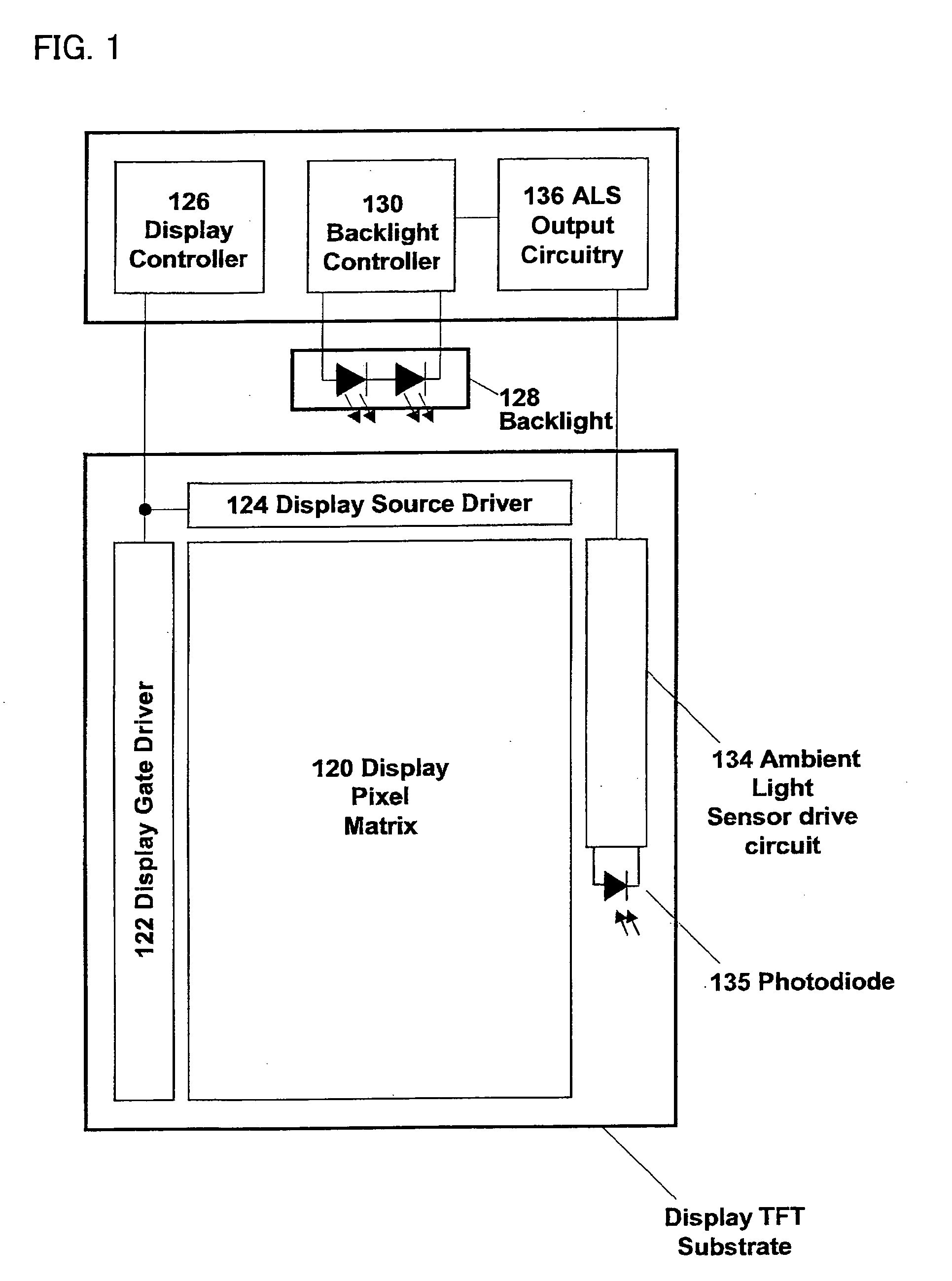
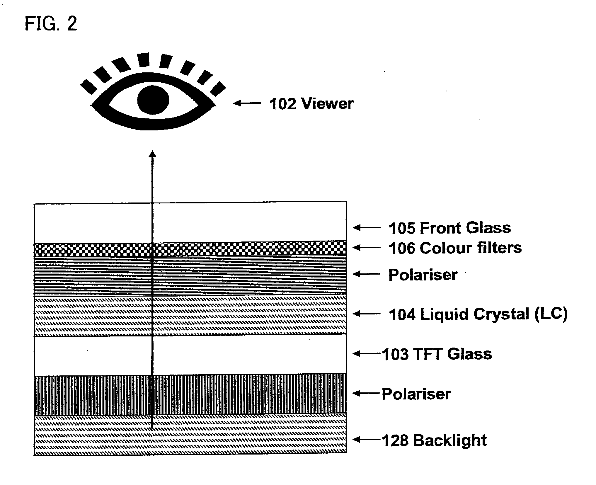
TECHNICAL FIELD[0001]The present invention relates to spectrally compensating a light sensor, for example a light sensor of an Ambient Light Sensor (ALS) system. The invention may be applied to a light sensor that is integrated into an active matrix liquid crystal display (AMLCD).[0002]This invention finds particular application in the integration of an ambient light sensor (ALS) on an AMLCD display substrate (shown FIG. 1).BACKGROUND ART[0003]FIG. 2 shows a simplified cross-section of a typical AMLCD. The backlight 128 is a light source used to illuminate the display. As is conventional, the display comprises a layer 104 of liquid crystal material disposed between transparent (eg glass) substrates 103, 105. Polarisers are provided, one on each side of the liquid crystal layer. The transmission of light through the display, from the backlight 128 to the viewer 102, is controlled by the use of electronic circuits made from thin film transistors (TFTs). The TFTs are fabricated on a gl...

Claims


Application Information

Patent Timeline
Patent Type & Authority Applications(United States)
IPC IPC(8): G09G5/00
CPCG01J1/1626G01J1/32G01J1/4204G01J3/51H05B33/0803G09G3/3406G09G2320/0626G09G2360/144G01J3/513Y02B20/40H05B47/11H05B45/12G01J3/50G09G3/3413H05B45/30
Inventor HADWEN, BENJAMIN JAMES
Owner SHARP KK
Learn More