Method for fabricating a semi-polar nitride semiconductor

Inactive Publication Date: 2011-02-24
NAT CENT UNIV
View PDF5 Cites 20 Cited by
  • Summary
  • Abstract
  • Description
  • Claims
  • Application Information

AI Technical Summary

Benefits of technology

[0007]A primary objective of the present invention is to provide a method for fabricating a semi-polar nitride semiconductor, whereby a buffer layer is used to improve the quality of a semi-polar nitride semiconductor formed on a (001) substrate t

Problems solved by technology

Therefore, silicon atoms will not diffuse into the GaN material, thus solving the problems of the back-melting etching ph

Method used


Image

  • Method for fabricating a semi-polar nitride semiconductor
  • Method for fabricating a semi-polar nitride semiconductor
  • Method for fabricating a semi-polar nitride semiconductor

Examples


Embodiment Construction

[0014]The fabricating process of the present invention is described by using the silicon substrate as an example, but the scope of the present invention is not so limited. In other words, the present invention is not only suited to the silicon substrate, but also suitable to substrate made of other materials.

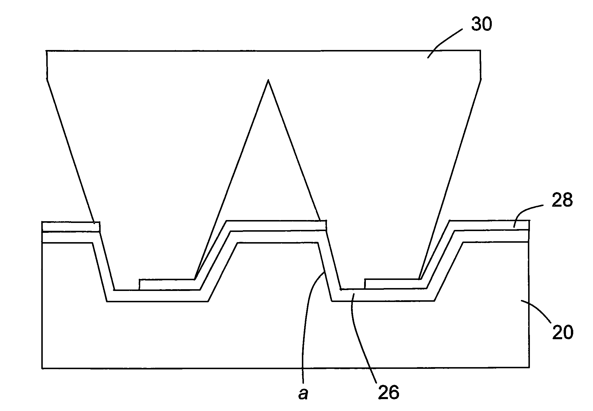
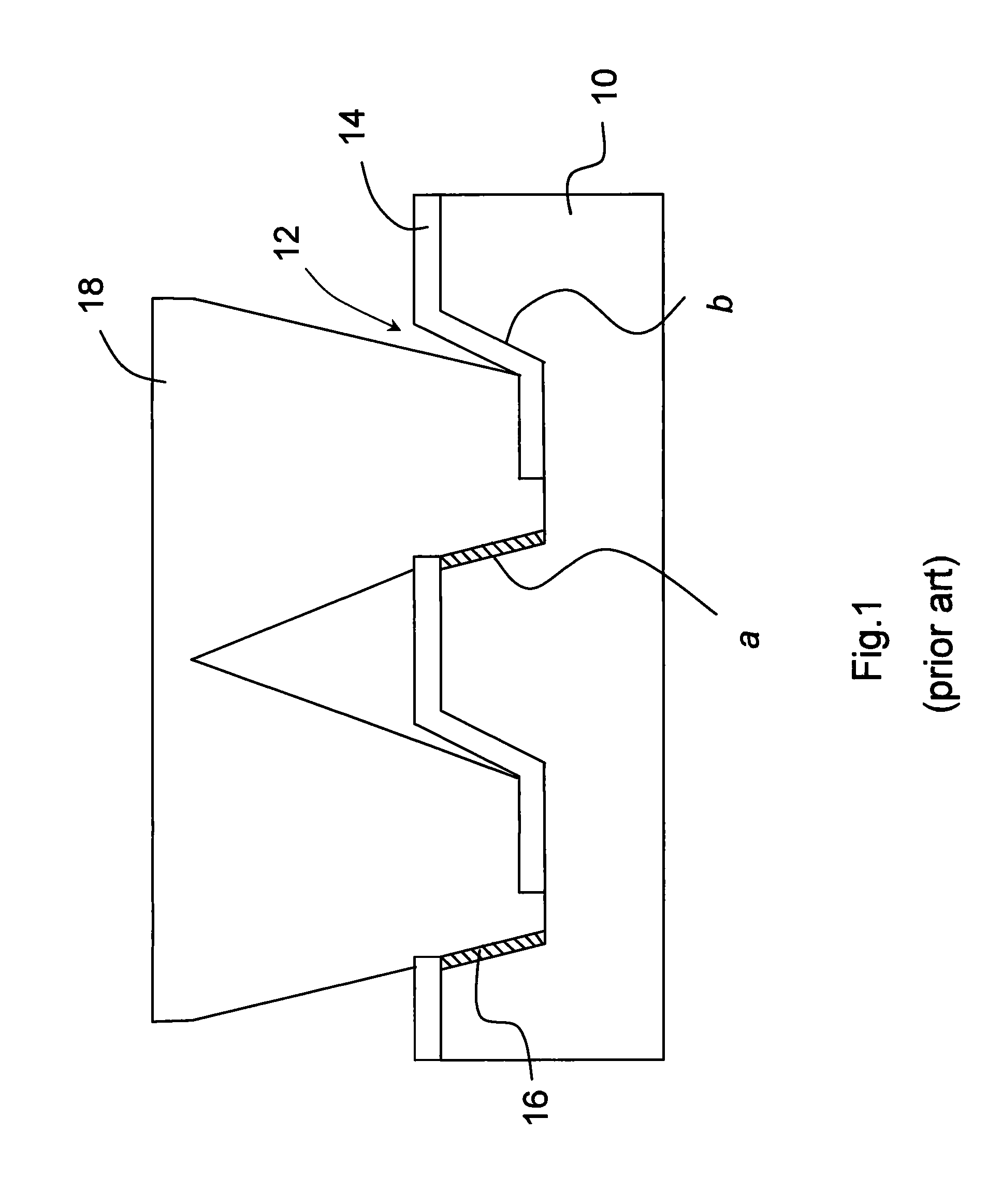
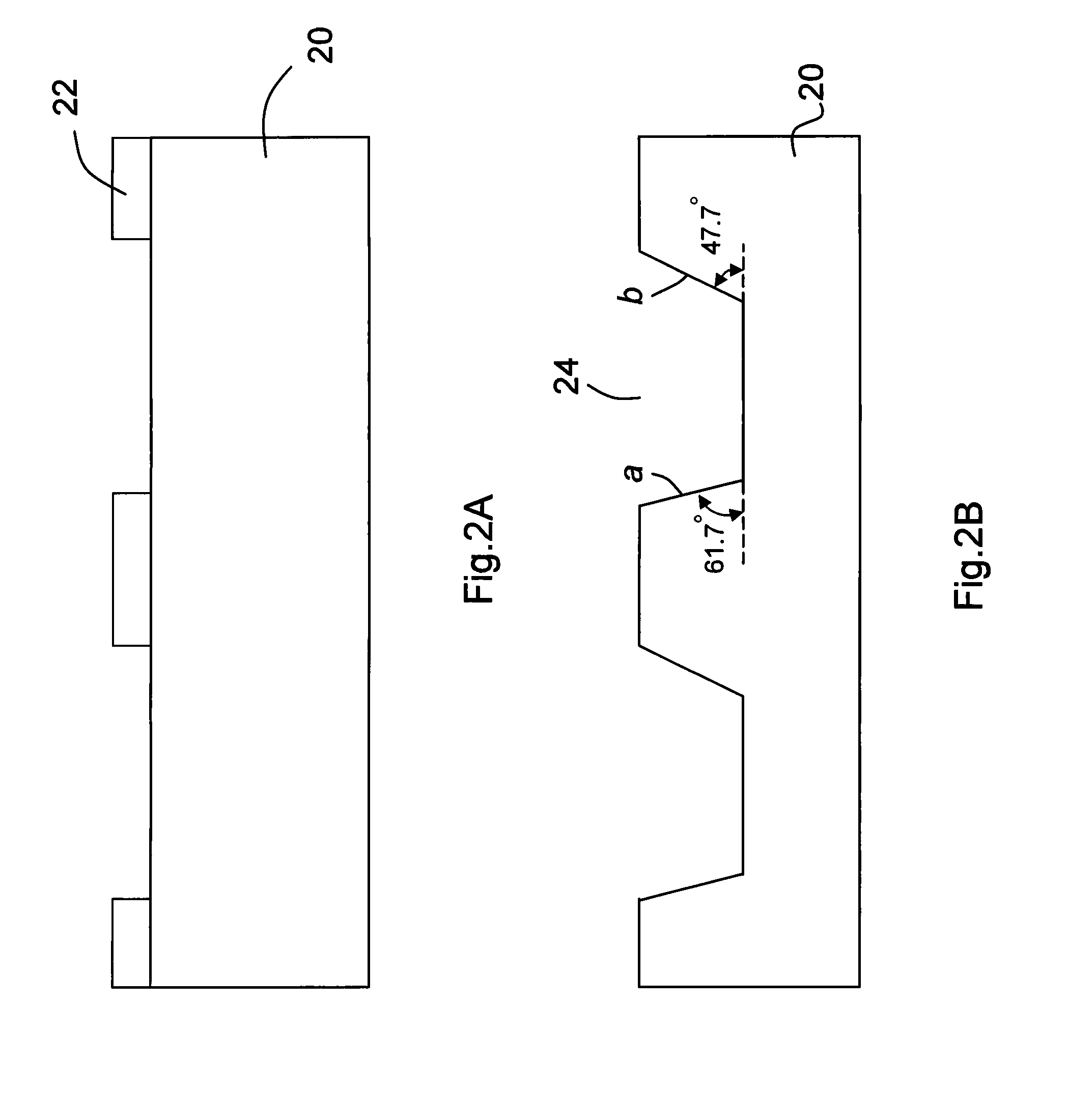
[0015]Refer to FIGS. 2A-2E for diagrams schematically showing the steps of a method for fabricating the semi-polar nitride semiconductor according to the embodiment of the present invention. As shown in FIG. 2A, a silicon dioxide ridge-like periodical mask pattern 22, which is parallel to a 110 direction is formed on a (100) silicon substrate 20 tilted at 7 degrees by using the exposure and development processes. Next, as shown in FIG. 2B, the silicon substrate 20 exposed through the mask pattern 22 is etched to form V-like grooves 24 by using a etching solution, wherein tilted surfaces of the V-like groove 24 are a (111) surface a at 61.7 degrees and a ( 111) surface b at 47.7 ...


PUM


Abstract

A method for fabricating a semi-polar nitride semiconductor is disclosed, comprising following steps: firstly, a (001) substrate tilted at 7 degrees and having a plurality of V-like grooves is provided, and tilted surfaces of the V-like groove are a (111) surface at 61.7 degrees and a ( 111) surface at 47.7 degrees; next, a surface of said substrate is cleaned by using a deoxidized solution, and then a buffer layer is formed on said substrate to cover said V-like grooves; then, said buffer layer is covered with an oxide layer except for said buffer layer formed on said (111) surface at 61.7 degrees; and finally, said semi-polar nitride semiconductor is formed on said buffer layer having (111) surface at 61.7 degrees to enhance the quality of said semi-polar nitride semiconductor.

Description

BACKGROUND OF THE INVENTION[0001]1. Field of the Invention[0002]The present invention relates to a method for fabricating semi-polar nitride semiconductor, particularly to a method for fabricating semi-polar nitride semiconductor by using the characteristics of a buffer layer to enhance the quality of the semi-polar nitride semiconductor.[0003]2. Description of the Related Art[0004]The traditional semi-polar nitride semiconductor is like gallium nitride (GaN), which forms on the silicon substrate having periodical V-like grooves. Refer to FIG. 1 for a diagram schematically showing the semi-polar nitride semiconductor formed on a substrate according to the prior art. As shown in FIG. 1, the first step of forming the semi-polar nitride semiconductor is to form a silicon dioxide ridge-like periodical mask pattern, which is parallel to a 110 direction on a (001) silicon substrate 10 tilted at 7 degrees. Next, the substrate 10 is etched to have V-like grooves 12 by using a potassium hydr...

Claims


Application Information

Patent Timeline
IPC IPC(8): H01L21/20
CPCC30B25/183C30B25/186C30B29/403H01L21/02381H01L21/02639H01L21/02433H01L21/02472H01L21/0254H01L21/0243
Inventor LIU, HSUEH-HSINGCHYI, JEN-INNWU, CHIN-CHI
Owner NAT CENT UNIV
Why Eureka
Try Eureka