Semiconductor device, method of manufacturing semiconductor device, and lead frame thereof

a semiconductor device and semiconductor technology, applied in semiconductor devices, semiconductor/solid-state device details, electrical apparatus, etc., can solve the problems of increased difficult to follow electric signals, and difficult to reduce the size of photo-couplers, so as to prevent the manufacturing cost of semiconductor devices from increasing, the coupling coefficient of inductors is raised.

Inactive Publication Date: 2011-03-03
RENESAS ELECTRONICS CORP
View PDF17 Cites 61 Cited by
  • Summary
  • Abstract
  • Description
  • Claims
  • Application Information

AI Technical Summary

Benefits of technology

[0018]According to the invention, in the semiconductor device performing the signal transmission between the first semiconductor chip and the second semiconductor chip using the induction coupling of the inductors, it is possible to prevent the manufacturing cost of the semiconductor device from increasing while raising the coupling coefficient of the inductors.

Problems solved by technology

However, since the photo-coupler has a light emitting element and a light receiving element, it is difficult to reduce the photo-coupler in size.
When a frequency of an electric signal is high, it is difficult to follow the electric signal.
When the semiconductor substrate is provided with the through-hole, the manufacturing cost of the semiconductor device is increased.
As described above, it is difficult to raise the coupling coefficient between inductors while decreasing the manufacturing cost of the semiconductor device.

Method used


Image

  • Semiconductor device, method of manufacturing semiconductor device, and lead frame thereof
  • Semiconductor device, method of manufacturing semiconductor device, and lead frame thereof
  • Semiconductor device, method of manufacturing semiconductor device, and lead frame thereof

Examples


first embodiment

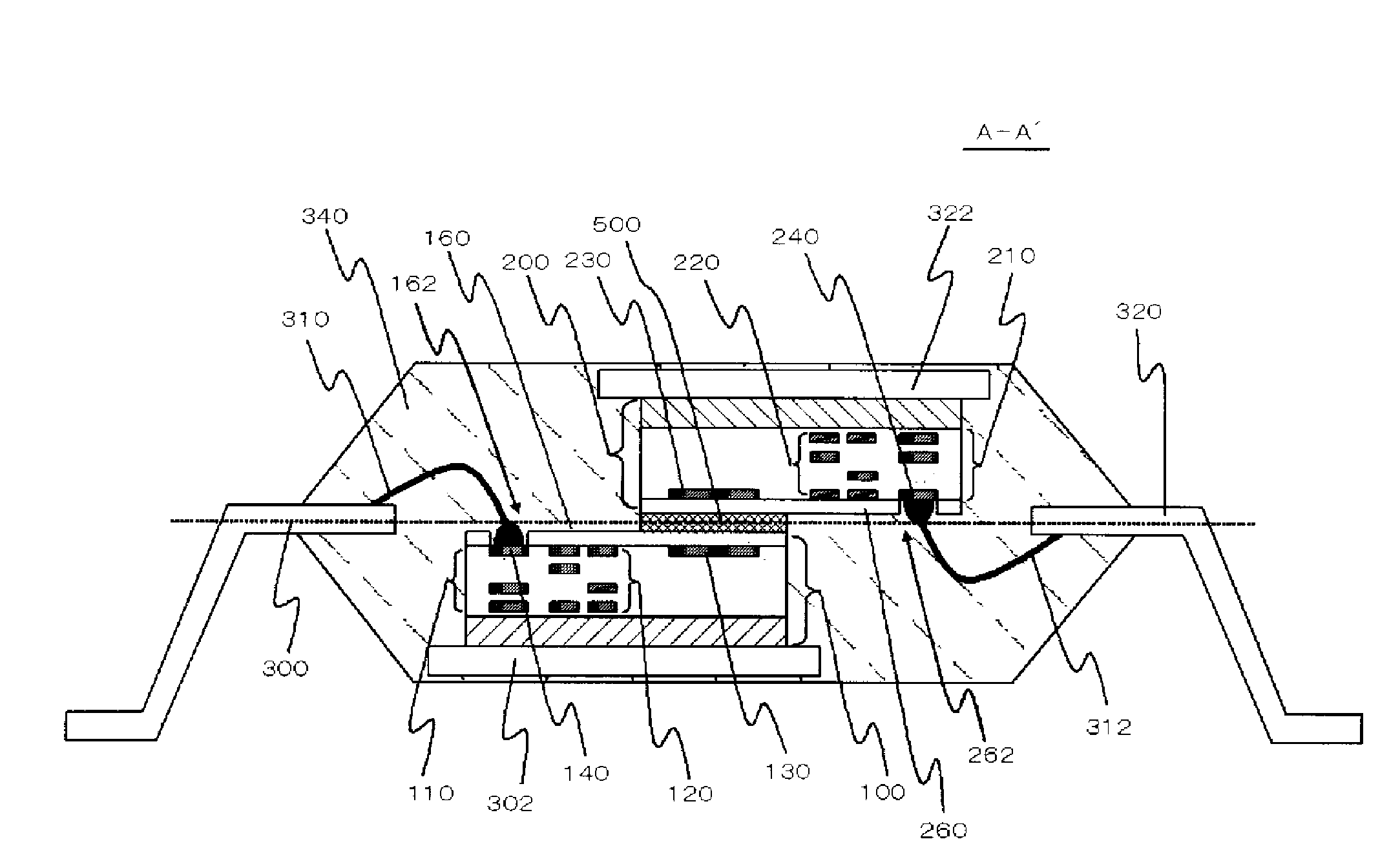
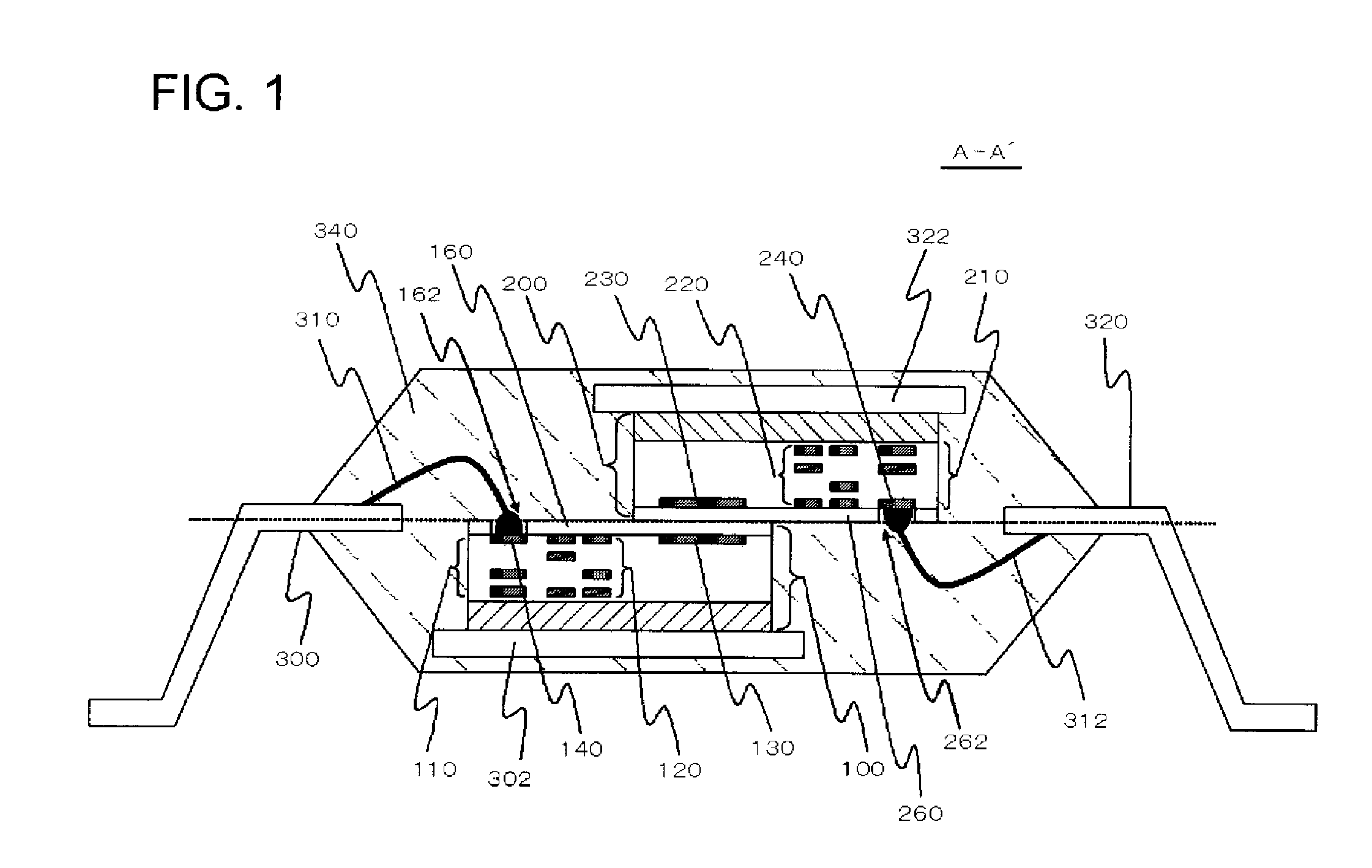
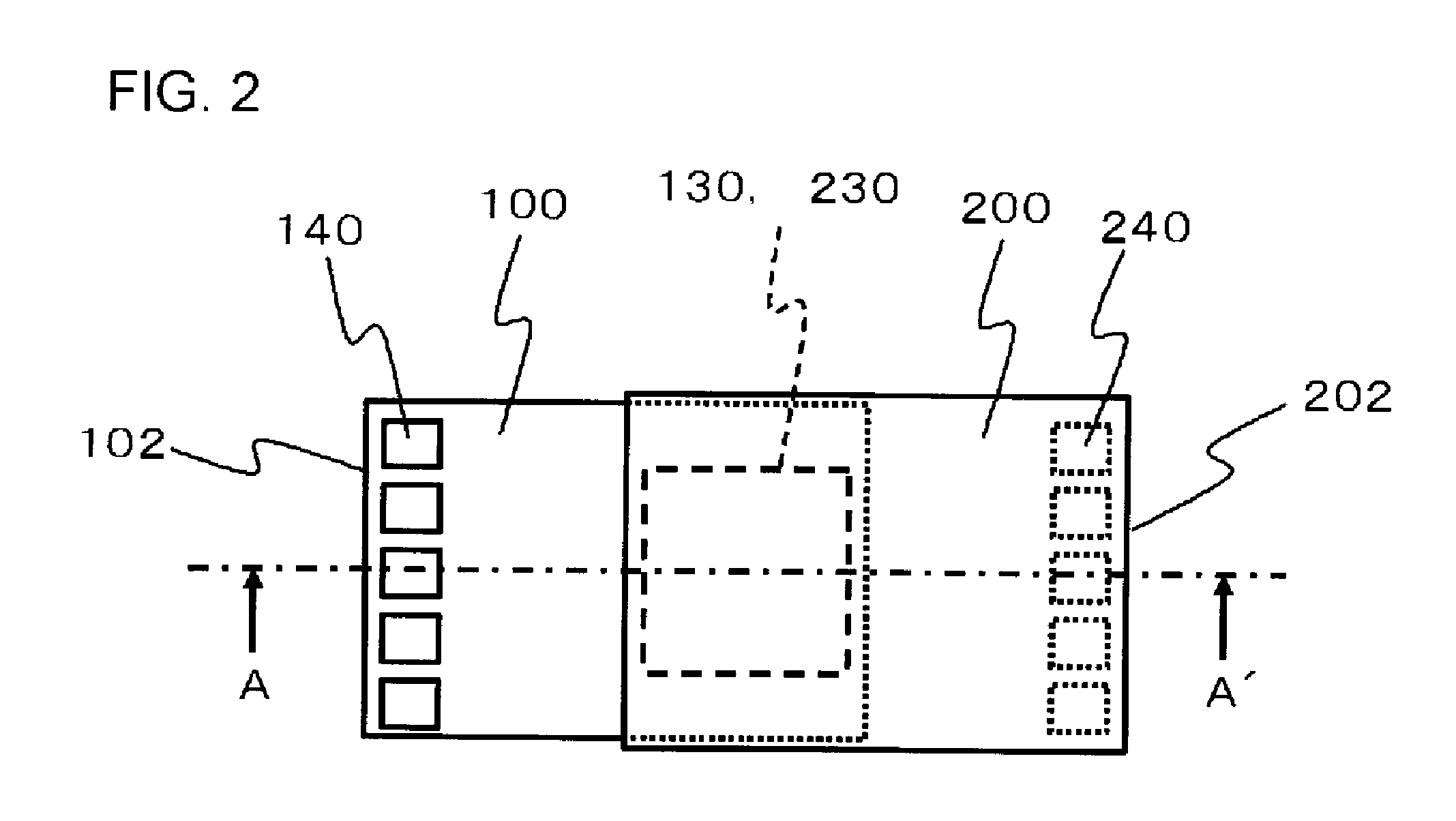
[0047]FIG. 1 is a cross-sectional view illustrating a configuration of a semiconductor device according to a The semiconductor device has a first semiconductor chip 100 and a second semiconductor chip 200. The first semiconductor chip 100 has a first multilayer interconnect layer 110 and a first inductor 130. The first inductor 130 is formed in the first multilayer interconnect layer 110. The second semiconductor chip 200 has a second multilayer interconnect layer 210 and a second inductor 230. The second inductor 230 is formed in the second multilayer interconnect layer 210. The first semiconductor chip 100 and the second semiconductor chip 200 are overlapped in a direction in which the first multilayer interconnect layer 110 and the second multilayer interconnect layer 210 are opposed to each other. When seen in a plan view, the first inductor 130 and the second inductor 230 are overlapped. The first semiconductor chip 100 and the second semiconductor chip 200 have non-opposed ar...

second embodiment

[0081]According to the embodiment, the same advantages as the first or second embodiment can be obtained.

[0082]FIG. 11 is a plan view of a semiconductor device according to a fourth embodiment, and corresponds to FIG. 10 of the third embodiment. The semiconductor device according to the embodiment has the same configuration as the semiconductor device according to the third embodiment, except that the first semiconductor device 100 and the second semiconductor device 200 obliquely deviate when seen in a plan view.

[0083]According to the embodiment, the same advantages as the first or second embodiment can be obtained.

[0084]FIG. 12 is a cross-sectional view of a semiconductor device according to a fifth embodiment, and corresponds to FIG. 1 of the first embodiment. The semiconductor device according to the embodiment has the same configuration as the semiconductor device according to the first embodiment, except that the first inductor 130 is formed in an interconnect layer other than...

eighth embodiment

[0105]Then, as shown in FIG. 19, the second semiconductor chip 200 is mounted over the first semiconductor chip 100. The method of mounting the second semiconductor chip 200 is the same as the

[0106]Then, as shown in FIG. 20, the first semiconductor chip 100 and the lead 306 are connected to each other by the first bonding wire 310, and the second semiconductor chip 200 and the lead 308 are connected to each other by the second bonding wire 312. Processes thereafter are the same as described in the first embodiment. The leads 306 and 308 can be bent toward the first semiconductor chip 100.

[0107]According to the embodiment, the same advantages as the eighth embodiment can be obtained. When providing the bonding wire 312, the bonding wire 312 does not easily interfere with a stage of a bonding device due to the thickness of the die pad 322.

[0108]FIG. 21 is a cross-sectional view illustrating a configuration of a semiconductor device according to a tenth embodiment. The semiconductor de...


PUM


Abstract

A first semiconductor chip and a second semiconductor chip are overlapped with each other in a direction in which a first multilayer interconnect layer and a second multilayer interconnect layer are opposed to each other. When seen in a plan view, a first inductor and a second inductor are overlapped. The first semiconductor chip and the second semiconductor chip have non-opposed areas which are not opposed to each other. The first multilayer interconnect layer has a first external connection terminal in the non-opposed area, and the second multilayer interconnect layer has a second external connection terminal in the non-opposed area.

Description

[0001]This application is based on Japanese patent application No. 2009-203040, the content of which is incorporated hereinto by reference.BACKGROUND[0002]1. Technical Field[0003]The present invention relates to a semiconductor device performing signal transmission between a first semiconductor chip and a second semiconductor chip using induction coupling of inductors, a method of manufacturing the semiconductor device, and a lead frame thereof.[0004]2. Related Art[0005]When signals are transmitted between two semiconductor chips which are not in contact, there are many cases of using a photo-coupler (e.g., Japanese Laid-open patent publication NO. 2004-186297). However, since the photo-coupler has a light emitting element and a light receiving element, it is difficult to reduce the photo-coupler in size. When a frequency of an electric signal is high, it is difficult to follow the electric signal.[0006]Hereupon, recently, as described in Japanese Laid-open patent publication NOS. 2...

Claims


Application Information

Patent Timeline
Patent Type & Authority Applications(United States)
IPC IPC(8): H01L23/495H01L21/60
CPCH01L23/48H01L23/49537H01L23/49575H01L24/29H01L24/45H01L24/48H01L24/73H01L24/85H01L25/0657H01L2224/2919H01L2224/45147H01L2224/48091H01L2224/48247H01L2224/48465H01L2224/49171H01L2224/73215H01L2224/73265H01L2224/83101H01L2224/83855H01L2225/06562H01L2924/01004H01L2924/01014H01L2924/01028H01L2924/01029H01L2924/01047H01L2924/01082H01L2924/3025H01L24/32H01L2224/29H01L2224/29298H01L2224/32145H01L2224/32245H01L2924/01006H01L2924/01021H01L2924/01023H01L2924/01033H01L2924/0665H01L24/49H01L2924/0132H01L2224/85H01L23/49534H01L21/56H01L2924/00013H01L2224/29139H01L23/5227H01L23/544H01L23/645H01L2223/6655H01L2924/07802H01L2924/00014H01L2924/0635H01L2924/00H01L2924/01026H01L2924/00012H01L2224/29099H01L2224/29199H01L2224/29299H01L2224/2929H01L2924/181H01L2224/92147H01L2224/92247H01L2224/04042H01L2224/85399H01L2224/05599
Inventor NAKASHIBA, YASUTAKAOGAWA, KENTA
Owner RENESAS ELECTRONICS CORP
Why Eureka
Try Eureka