Flip-Chip Package Structure

a technology of flip-chip and package structure, which is applied in the direction of semiconductor devices, semiconductor/solid-state device details, electrical devices, etc., can solve the problems of affecting the packaging yield, the cladding material b>7/b> is often not fine enough, and the substrate area is saved, so as to prevent the risk of configuring voids, the effect of reducing the risk of voids

Inactive Publication Date: 2011-03-03
KINSUS INTERCONNECT TECH
View PDF3 Cites 90 Cited by
  • Summary
  • Abstract
  • Description
  • Claims
  • Application Information

AI Technical Summary

Benefits of technology

[0008]A primary objective of the present invention is to provide an FC package structure. The FC package structure includes a substrate, a chip, a plurality of copper platform bumps, a circuit pattern layer, a plating layer, and a solder mask layer. The copper platform bumps and the circuit pattern layer are disposed on the substrate. The copper platform bumps have a height higher than a height of the circuit pattern layer. Each copper platform bump includes a copper platform and a copper bump. The copper platform is stacked on the copper bump. The plating layer is plated on the copper platform bumps, for connecting with chip foot pad provided at a bottom of the chip. The FC package structure does not need to reserve a space for wire bonding and thus the area of the substrate can be saved, and the product can be made smaller.
[0009]Accordingly, the present invention is adapted for providing a solution of the problem of the conventional technology. According to the present invention, the copper platform bumps are configured with a height higher than the height of the circuit pattern layer. In such a way, the chip is blocked up, so that the gap between the chip and the substrate is enlarged, thus preventing the risk of configuring voids when filling the cladding material and improving the packaging yield.

Problems solved by technology

However, according to the conventional technology, the gap d1 is very small, and the stuff of the cladding material 7 is often not fine enough.
In such a way, a void may be configured beneath the chip 8, which adversely affects the packaging yield.

Method used


Image

  • Flip-Chip Package Structure
  • Flip-Chip Package Structure
  • Flip-Chip Package Structure

Examples


Embodiment Construction

[0019]The accompanying drawings are included to provide a further understanding of the invention, and are incorporated in and constitute a part of this specification. The drawings illustrate embodiments of the invention and, together with the description, serve to explain the principles of the invention.

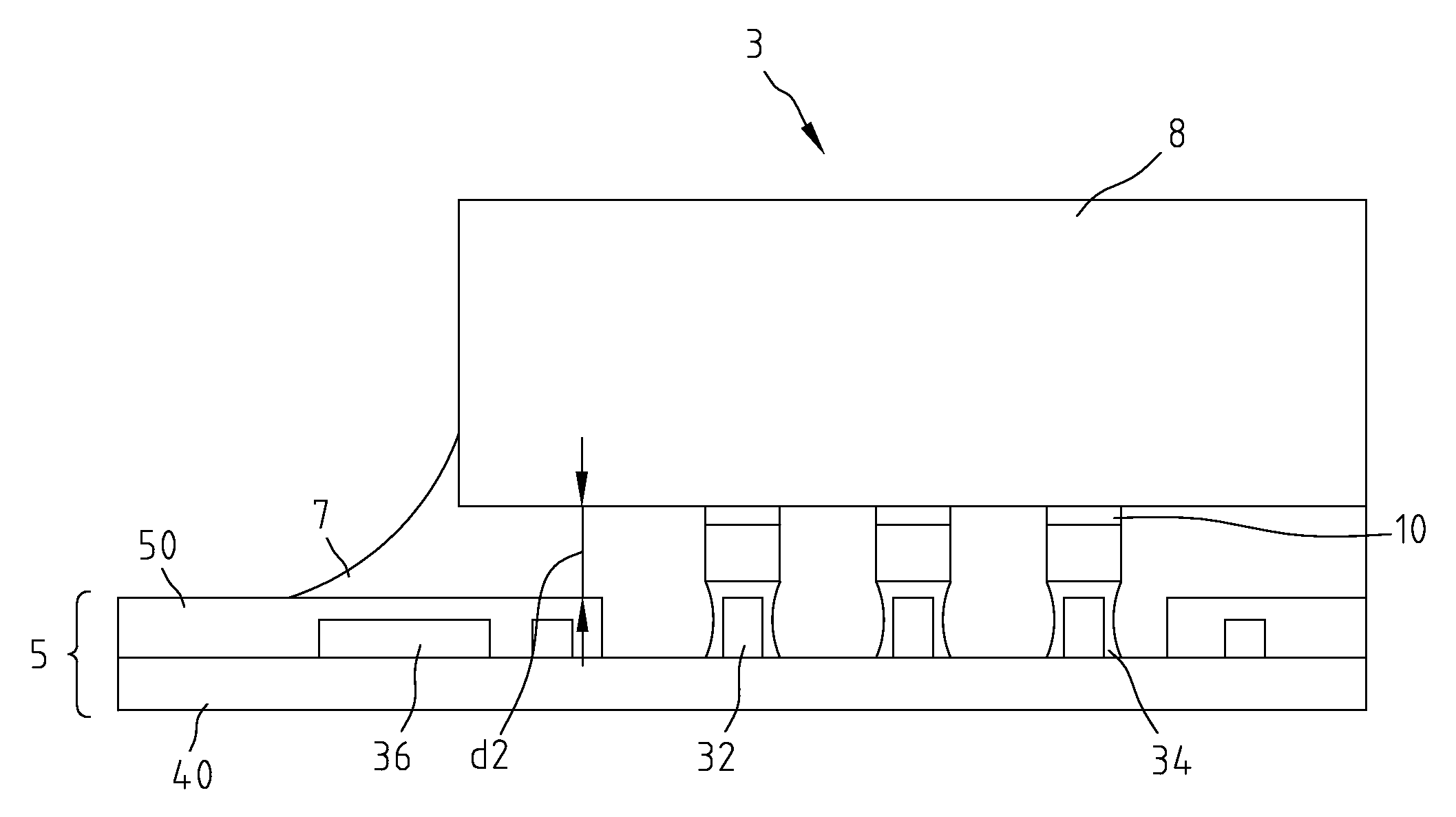
[0020]FIG. 5 is a schematic diagram illustrating an FC package structure of the present invention. Referring to FIG. 5, the present invention provides a flip-chip (FC) package structure 3. The FC package structure 3 includes a chip 8, an FC platform structure 5, and a cladding structure 7. The chip 8 includes a plurality of chip foot pads 10 disposed at a bottom of the chip 8. The FC platform structure 5 includes a substrate 40, a plurality of copper platform bumps 32, a plating layer 34, a circuit pattern layer 36, and a solder mask layer 50. The copper platform bumps 32 and the circuit pattern layer 36 are all disposed on an upper surface of the substrate 40. Each of the copper pla...


PUM


Abstract

A flip-chip (FC) package structure is provided. The FC package structure includes a substrate, a chip, a plurality of copper platforms, a plurality of copper bumps, a plating layer, a circuit layer and a solder mask layer. The copper bumps are disposed on the substrate. The copper platforms are stacked on the copper bumps. The plating layer covers the copper bumps and the copper platforms, for contacting with chip foot pads configured at a bottom of the chip. The FC package structure does not need to reserve a space for wire bonding, thus saving the area of the substrate. The copper platforms are stacked on the copper bumps, and are higher than the circuit pattern layer. Therefore, the chip is blocked up, and the gap between the chip and the substrate is enlarged, thus preventing the risk of configuring voids when filling the cladding material and improving the packaging yield.

Description

BACKGROUND OF THE INVENTION[0001]1. Field of the Invention[0002]The present invention relates generally to a flip-chip (FC) package structure, and more particularly, to an FC package structure configured with copper platform bumps.[0003]2. The Prior Arts[0004]FC packaging is a new generation of semiconductor packaging method. An FC package structure usually includes a substrate and a chip I / O. The substrate and the chip I / O are typically bonded one to another by welding to the wafer bump with tin and / or lead bumps provided on the substrate, for transmitting signals or power. The FC package structures were widely employed in fabricating chip products related to personal computers (PC), and are now more often used in fabricating chip package structures of handheld products such as mobile phones and MP3. Comparing with wire-bond type chip scale packaging method, which is conventionally and typically used for packaging the chips of present handheld consumer electronic products, gold stu...

Claims


Application Information

Patent Timeline
Patent Type & Authority Applications(United States)
IPC IPC(8): H01L23/498
CPCH01L23/49811H01L2224/13147H01L24/16H01L24/81H01L2224/13099H01L2224/16225H01L2224/81193H01L2224/81203H01L2224/81801H01L2924/01029H01L2924/01046H01L2924/01078H01L2924/01079H01L2924/01082H01L2924/01033H01L2924/0105H01L2924/014H01L24/13H01L2224/13144H01L2924/00014H01L2924/181H01L2924/00
Inventor HSU, JUN-CHUNGCHANG, SHUO-HSUN
Owner KINSUS INTERCONNECT TECH
Why Eureka
Try Eureka