Metallization layer of a semiconductor device having differently thick metal lines and a method of forming the same

a technology of metallization layer and semiconductor device, which is applied in the direction of semiconductor device, semiconductor/solid-state device details, electrical apparatus, etc., can solve the problems of inefficient application of copper and copper alloys on substrates in large amounts, and the difficulty of solving the problem of a plurality of metallization layers, so as to achieve efficient adjustment of the resistivity of the corresponding line, improve the effect of flexibility and high compatibility

Active Publication Date: 2009-09-22
TAIWAN SEMICON MFG CO LTD
View PDF39 Cites 5 Cited by
  • Summary
  • Abstract
  • Description
  • Claims
  • Application Information

AI Technical Summary

Benefits of technology

[0015]Generally, the present disclosure is directed to a technique that provides enhanced flexibility during the formation of conductive lines, such as metal lines, in that the resistivity of metal lines is to a certain degree decoupled from the lateral dimensions thereof without unduly contributing to process complexity and maintaining a high degree of compatibility with conventional process strategies. For this purpose, metal lines may be formed in different device regions having a different thickness, thereby providing the potential for efficiently adjusting the corresponding line resistivity on the basis of the respective thickness of the metal, while substantially avoiding or reducing an increase of lateral dimensions in areas requiring low resistivity metal lines. Consequently, for a given design of a metallization layer, the conductivity of metal lines in selected device regions may be increased for given design dimensions when the constraints with respect to the pitch to neighboring metal lines is less demanding, thereby increasing performance without consuming additional substrate area. On the other hand, in respective designs of metallization layers requiring low resistivity lines, which may be conventionally obtained by increasing the lateral dimensions of the metal lines, a corresponding reduction of lateral dimension for the same line resistance may save substrate area, thereby reducing the dimensions of the respective circuit or provide the potential for increasing circuit complexity without consuming additional substrate area.

Problems solved by technology

Due to the large number of circuit elements and the required complex layout of advanced integrated circuits, the electrical connections of the individual circuit elements are generally not established within the same level on which the circuit elements are manufactured.
The fabrication of a plurality of metallization layers entails extremely challenging issues to be solved, such as mechanical, thermal and electrical reliability of each metallization layer in the layer stack.
Despite these advantages, copper and copper alloys also exhibit a number of disadvantages regarding the processing and handling in a semiconductor facility.
For instance, copper may not be efficiently applied onto a substrate in larger amounts by well-established deposition methods, such as chemical vapor deposition (CVD), and also may not be effectively patterned by the usually employed anisotropic etch procedures.
Another problem in manufacturing a metallization layer is the fact that controversial properties of a single metallization layer within a die region may have to be met with respect to conductivity and minimum pitch between neighboring metal lines.
However, a corresponding increase in performance may be obtained at the cost of a significantly increased substrate area, thereby reducing the overall packing density of the semiconductor device 100.
Consequently, when metal lines of different packing density are required in different device regions within a single die area, the conventional technique for the formation of metallization layers may not efficiently allow a combination of low-resistivity metal lines in one region while providing closely spaced metal regions in another die region.

Method used


Image

  • Metallization layer of a semiconductor device having differently thick metal lines and a method of forming the same
  • Metallization layer of a semiconductor device having differently thick metal lines and a method of forming the same
  • Metallization layer of a semiconductor device having differently thick metal lines and a method of forming the same

Examples


Embodiment Construction

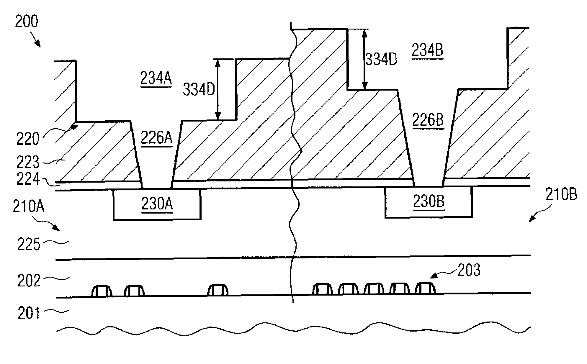
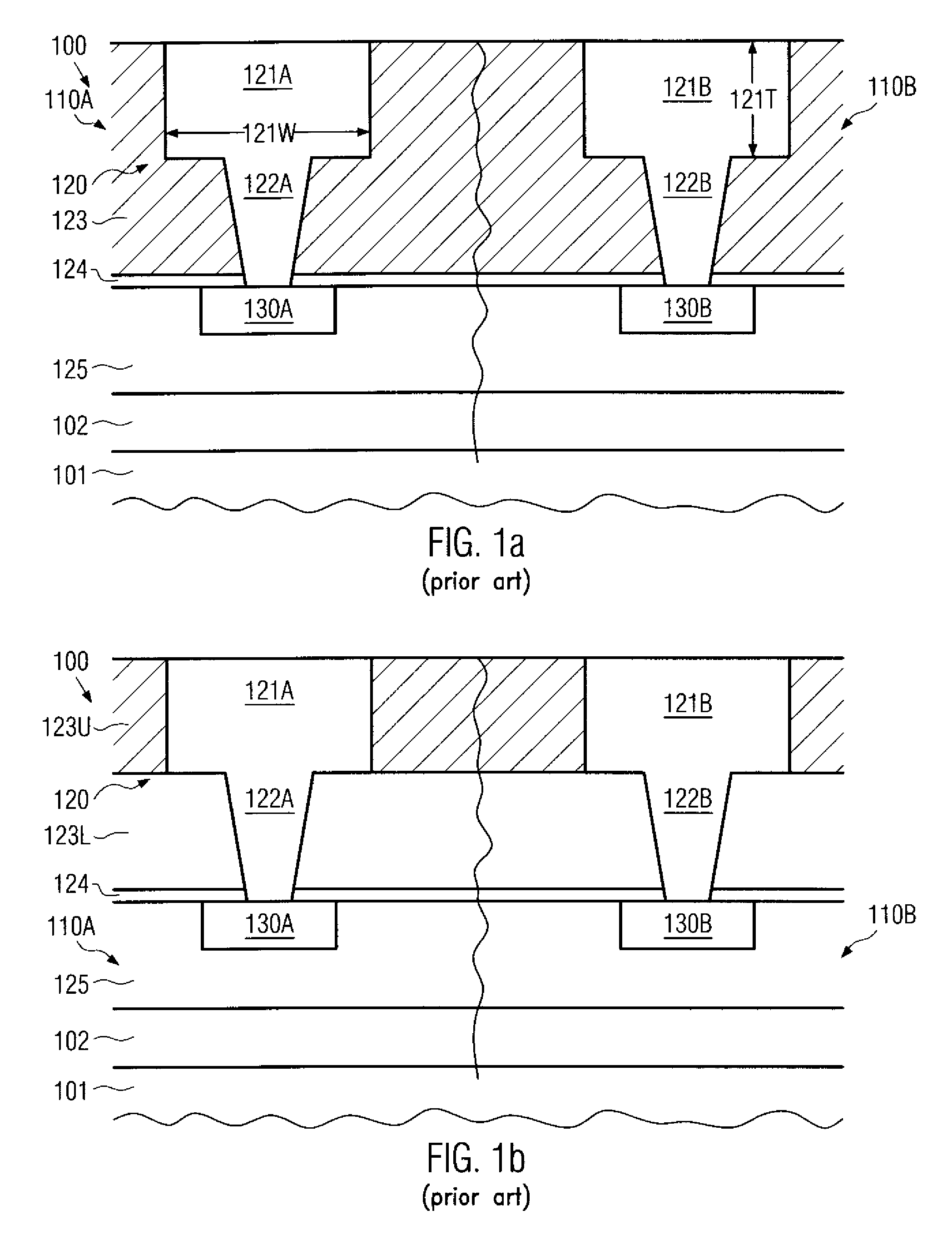
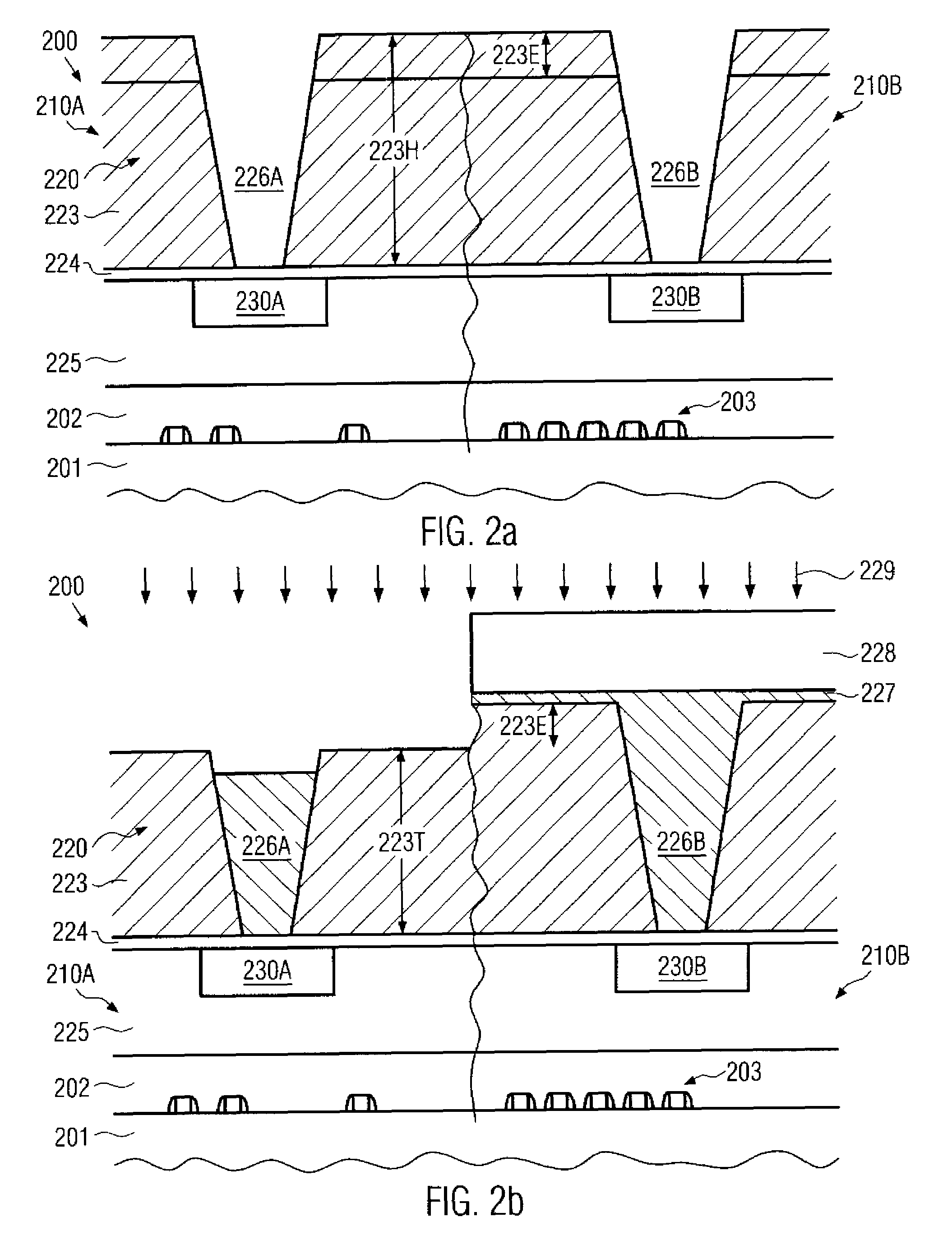
[0026]Illustrative embodiments of the invention are described below. In the interest of clarity, not all features of an actual implementation are described in this specification. It will of course be appreciated that in the development of any such actual embodiment, numerous implementation-specific decisions must be made to achieve the developers' specific goals, such as compliance with system-related and business-related constraints, which will vary from one implementation to another. Moreover, it will be appreciated that such a development effort might be complex and time-consuming, but would nevertheless be a routine undertaking for those of ordinary skill in the art having the benefit of this disclosure.

[0027]The present invention will now be described with reference to the attached figures. Various structures, systems and devices are schematically depicted in the drawings for purposes of explanation only and so as to not obscure the present invention with details that are well ...


PUM

PropertyMeasurementUnit
relative permittivityaaaaaaaaaa
dielectric constantaaaaaaaaaa
excess heightaaaaaaaaaa

Abstract

A semiconductor device comprises metal lines in a specific metallization layer which have a different thickness and thus a different resistivity in different device regions. In this way, in high density areas of the device, metal lines of reduced thickness may be provided in order to comply with process requirements for achieving a minimum pitch between neighboring metal lines, while in other areas having less critical constraints with respect to minimum pitch, a reduced resistivity may be obtained at reduced lateral dimensions compared to conventional strategies. For this purpose, the dielectric material of the metallization layer may be appropriately patterned prior to forming respective trenches or the etch behavior of the dielectric material may be selectively adjusted in order to obtain differently deep trenches.

Description

BACKGROUND OF THE INVENTION[0001]1. Field of the Invention[0002]Generally, the present disclosure relates to the formation of integrated circuits, and, more particularly, to the formation of metallization layers including highly conductive metals, such as copper, embedded into a dielectric material.[0003]2. Description of the Related Art[0004]In an integrated circuit, a very large number of circuit elements, such as transistors, capacitors, resistors and the like, are formed in or on an appropriate substrate, usually in a substantially planar configuration. Due to the large number of circuit elements and the required complex layout of advanced integrated circuits, the electrical connections of the individual circuit elements are generally not established within the same level on which the circuit elements are manufactured. Typically, such electrical connections are formed in one or more additional “wiring” layers, also referred to as metallization layers. These metallization layers ...

Claims


Application Information

Patent Timeline
Patent Type & Authority Patents(United States)
IPC IPC(8): H01L21/4763
CPCH01L21/76808H01L21/76816H01L21/76817H01L21/7684H01L21/76826H01L21/76835H01L21/76825H01L23/5283
Inventor LEHR, MATTHIASSCHALLER, MATTHIASPETERS, CARSTEN
Owner TAIWAN SEMICON MFG CO LTD
Why Eureka
Try Eureka