Page based management of flash storage

Inactive Publication Date: 2011-03-03
PIONEER CHIP TECH
View PDF9 Cites 376 Cited by
  • Summary
  • Abstract
  • Description
  • Claims
  • Application Information

AI Technical Summary

Benefits of technology

[0034]In a wearleveling process, an erased block has its erasure count compared to a sliding window that is a lowest block erasure count plus a block erasure count threshold. If the erased block count falls outside the sliding window is exceeded, a block having a lowest erased co

Problems solved by technology

The structure of a NAND flash memory chip does not permit reading and writing in a byte per byte basis but can only be accomplished in chunks of one page (typically 4 kb).
Additionally, an already written page cannot be overwritten.
The different unit size for read/write (1 page) and erase (64/128 pages) makes management of flash RAM chips difficult.
This also means random write of small chunks of data is quite slow, because blocks must be erased and data of the old

Method used


Image

  • Page based management of flash storage
  • Page based management of flash storage
  • Page based management of flash storage

Examples


Embodiment Construction

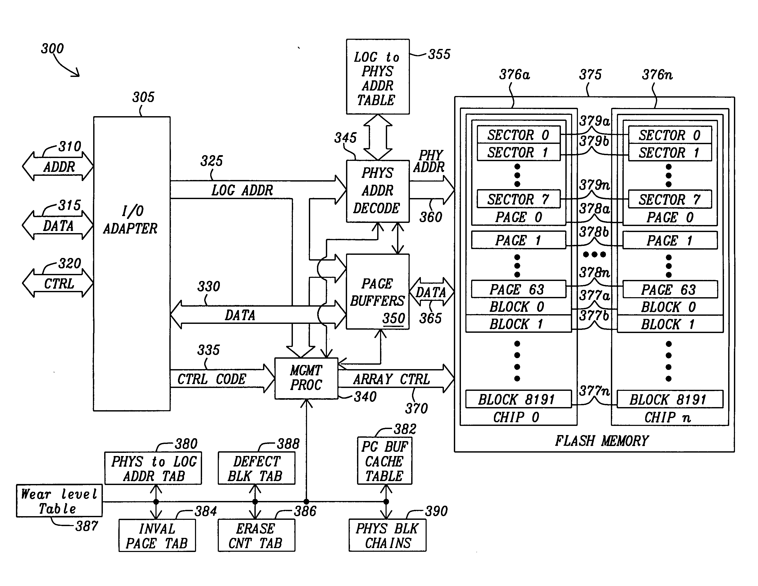
[0049]The page based management scheme of this invention decodes the address to index a logical-to-physical translation table to a page number within a block. The logical-to-physical translation table contains a cache residence bit to indicate if the page is resident in the page or must be retrieved from the array of Flash RAM nonvolatile memory devices.

[0050]If the page is not resident in the page buffer, it is fetched from the array of Flash RAM nonvolatile memory devices and placed in the page buffer. The sectors are read from or written to the page buffer as indicated by the low order address. If there are an insufficient amount of free pages within the page buffer, an eviction process evicts a least recently used page from the page buffer. If it is valid and is consistent with the page as stored in the array of Flash RAM nonvolatile memory devices, the page buffer page space is declared and the page is fetched from the array of Flash RAM nonvolatile memory devices. The sectors ...


PUM


Abstract

Methods and circuits for page based management of an array of Flash RAM nonvolatile memory devices provide paged base reading and writing and block erasure of a flash storage system. The memory management system includes a management processor, a page buffer, and a logical-to-physical translation table. The management processor is in communication with an array of nonvolatile memory devices within the flash storage system to provide control signals for the programming of selected pages, erasing selected blocks, and reading selected pages of the array of nonvolatile memory devices.

Description

BACKGROUND OF THE INVENTION[0001]1. Field of the Invention[0002]This invention relates generally to memory management systems and methods. More particularly, this invention relates to memory management circuits and methods for management of nonvolatile memory devices. Even more particularly, this invention relates to page based memory management of nonvolatile memory devices such as Flash Random Access Memory (RAM).[0003]2. Description of Related Art[0004]A solid-state drive (SSD) is a data storage device that uses semiconductor memory devices to store persistent data. An SSD is used to emulate a magnetic or electro-optical hard disk drive. The SSD employs an interface such as the Serial Advanced Technology Attachment (SATA) that allows the SSD to easily replace a hard disk drive in most applications. Other interface formats that may used by the SSD include Parallel Advanced Technology Attachment (PATA), Universal Serial Bus (USB), Peripheral Component Interconnect Express (PCI expr...

Claims


Application Information

Patent Timeline
IPC IPC(8): G06F12/00G06F12/02
CPCG06F12/0246G06F2212/7208G06F2212/7203G06F12/123
Inventor KUEHNE, REINHARD
Owner PIONEER CHIP TECH
Why Eureka
Try Eureka