Physical quantity sensor, manufacturing method of physical quantity sensor, and electronic apparatus

a manufacturing method and sensor technology, applied in the direction of speed/acceleration/shock measurement, flexible microstructure devices, instruments, etc., can solve the problems of difficult substrate use, complex manufacturing process of mems sensor, and inability to secure a path for providing direct-current bias or a path for taking out detection signals between capacitive electrodes only by, so as to reduce the cost of physical quantity sensors and provide physical quantity sensors relatively easily

Inactive Publication Date: 2011-03-10
SEIKO EPSON CORP
View PDF4 Cites 13 Cited by
  • Summary
  • Abstract
  • Description
  • Claims
  • Application Information

AI Technical Summary

Benefits of technology

[0007]An advantage of some aspects of the invention is to provide a physical quantity sensor (MEMS sensor) relatively easi

Problems solved by technology

However, in the MEMS sensor disclosed in JP-A-2007-150098, since the SOI substrate is expensive, there has been a problem that it is difficult to employ the substrate when the lower cost of the MEMS sensor is strongly desired.
Further, in the MEMS sensor disclosed in JP-T-2002-510139, when the trench isolation is provided on the silicon substrate, the manufacturing process of the MEMS sensor may become complex.
On the side surfaces facing ea

Method used


Image

  • Physical quantity sensor, manufacturing method of physical quantity sensor, and electronic apparatus
  • Physical quantity sensor, manufacturing method of physical quantity sensor, and electronic apparatus
  • Physical quantity sensor, manufacturing method of physical quantity sensor, and electronic apparatus

Examples


first embodiment

[0092]First, one configuration example of an MEMS sensor as a physical quantity sensor will be explained.

Overall Configuration of Capacitive Acceleration Sensor

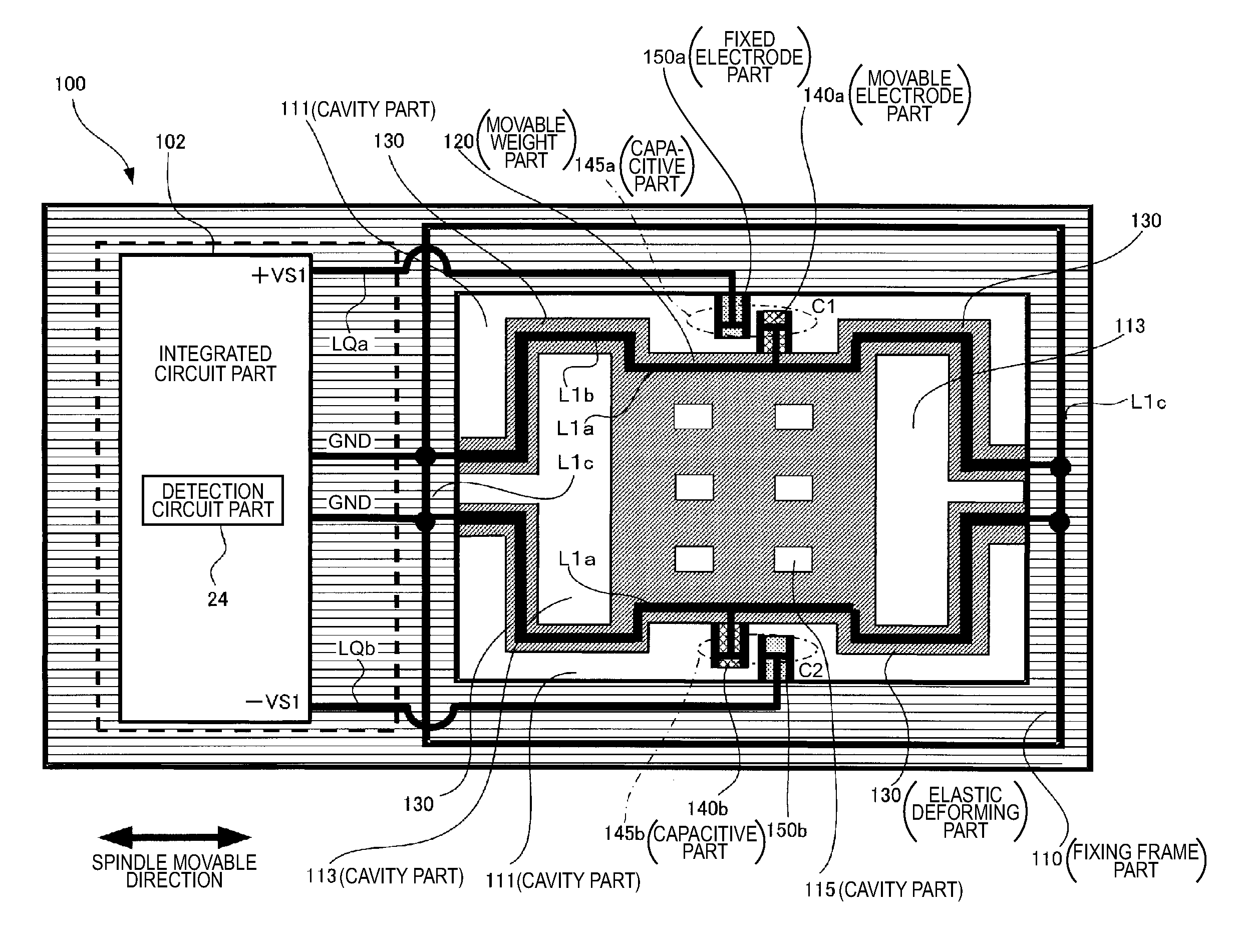
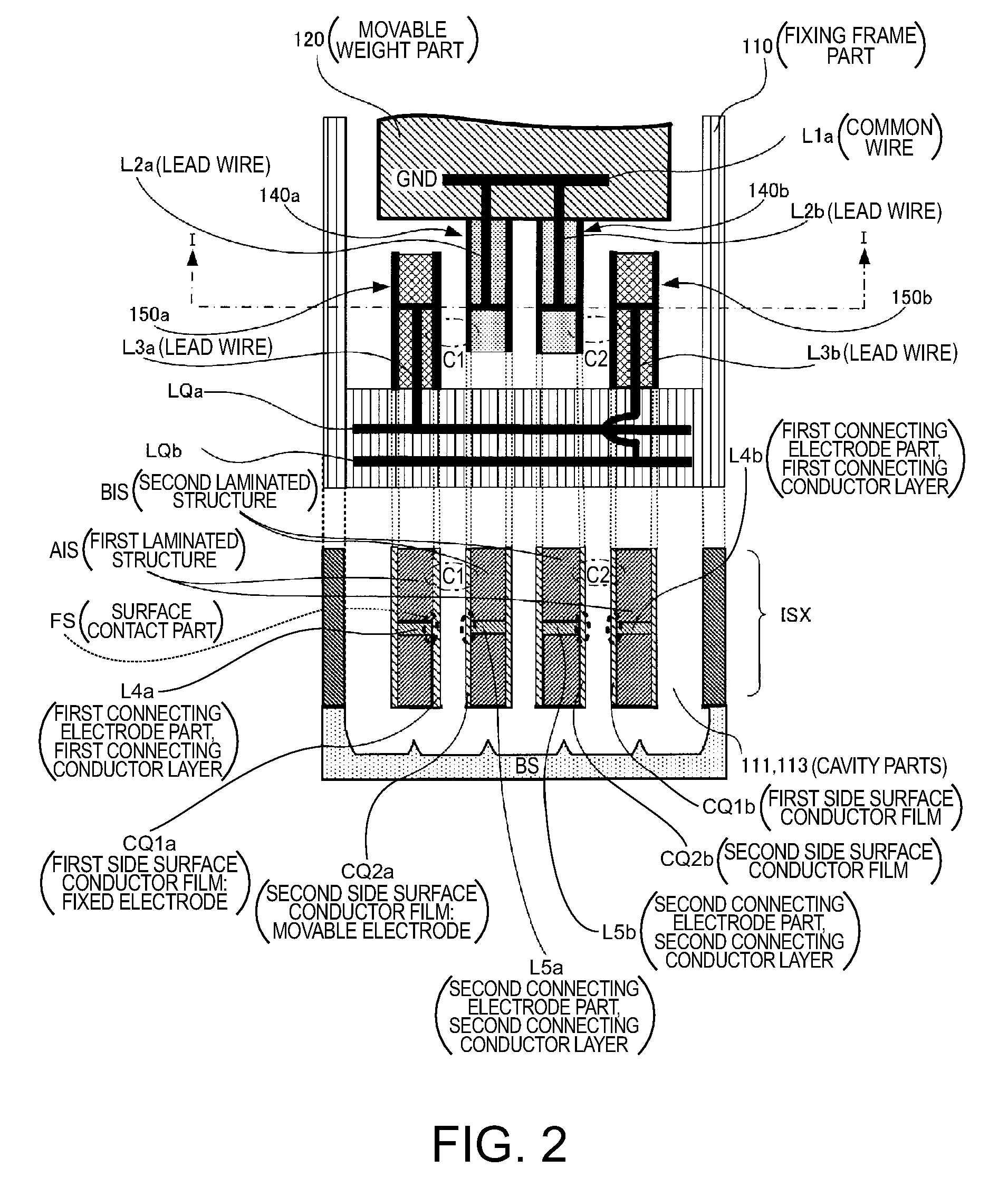
[0093]FIG. 1 is a plan view showing a configuration of an example of the MEMS sensor as a physical quantity sensor (here, a capacitive acceleration sensor) of an aspect of the invention. In the drawing, wires and electrodes formed by conducting materials are shown by thick solid lines.

[0094]In FIG. 1, a capacitive acceleration sensor 100 may be manufactured by forming a laminated structure on a substrate and selectively processing the laminated structure and the substrate using a semiconductor manufacturing technology. For example, after the laminated structure is formed on the substrate, the laminated structure is selectively patterned using anisotropic dry etching, for example, to form cavity parts 111, 113, 115, and further, an etchant for isotropic etching is allowed to reach the substrate surface via the cavity parts 111...

first example

[0115]FIGS. 3A to 3F are diagrams (sectional views of a device) for explanation of an outline of a basic manufacturing process (first example) of an MEMS sensor like the capacitive acceleration sensor 100 shown in FIGS. 1 and 2.

[0116]At the first step shown in FIG. 3A, the laminated structure ISX in which the insulating layers, at least one conductor layer QL (for example, the conductor layer to be the first connecting conductor layers L4a, L4b as the first connection electrode part, the second connecting conductor layers L5a, L5b as the second connection electrode part, the lead wires L2a, L2b, L3a, L3b, etc.) are formed is formed on the substrate BS.

[0117]At the second step shown in FIG. 3B, the laminated structure ISX formed on the substrate BS is patterned by anisotropic etching and a first cavity part Opa (specifically, the first cavity parts 111a, 113a, 115a) is formed. The at least one conductor layer QL is patterned, and thereby, the first connecting conductor layers L4a, L4...

second example

[0124]FIGS. 19A to 21C are sectional views of a device with respect to each step for explanation of an outline of a manufacturing method (second example) of the capacitive acceleration sensor 100 shown in FIGS. 1 and 2.

[0125]In the manufacturing method of the capacitive acceleration sensor 100 shown in FIGS. 19A to 21C, when the fixed electrode (the first side surface conductor CQ1) is formed in the fixed electrode part 150 and the movable electrode (second side surface conductor CQ2) is formed in the movable electrode part 140, a method of securing electric conduction via contact conductors (connecting conductors) formed to cover the bottom surfaces and the inner wall surfaces of contact holes is employed.

[0126]That is, at the first step shown in FIG. 19A, a conductor layer as the first connecting electrode part (first internal conductor: here, referred to as “LX1” for convenience of explanation) is embedded in the laminated structure ISX. The end of the first internal conductor LX...


PUM


Abstract

A physical quantity sensor includes: a fixing part; an elastic deforming part; a movable weight part coupled to the fixing part via the elastic deforming part; a fixed arm part extended from the fixing part; and a movable arm part extended from the movable weight part and provided to face the fixed arm part via a gap, wherein the fixed arm part and the movable arm part are laminated structures containing insulating layers and conductor layers, the fixed arm part has a first side surface conductor film provided on a side surface of the fixed arm part and a first connecting electrode part using the conductor layer and electrically connected to the first side surface conductor film, and the movable arm part has a second side surface conductor film provided on aside surface opposed to the first side surface conductor film and a second connecting electrode part using the conductor layer and electrically connected to the second side surface conductor film.

Description

BACKGROUND[0001]1. Technical Field[0002]The present invention relates to a physical quantity sensor such as an MEMS sensor (Micro Electro Mechanical Sensor), for example, a manufacturing method of a physical quantity sensor, an electronic apparatus having a physical quantity sensor, etc.[0003]2. Related Art[0004]A capacitive MEMS sensor as a physical quantity sensor manufactured using a semiconductor manufacturing technology is disclosed in JP-A-7-301640, for example. For the MEMS sensor, a structure including silicon (Si) is generally used. The silicon is not an insulating material, and thus, the component part having continuous silicon is electrically conductive. Accordingly, for capacity detection, electric separation in some way is necessary.[0005]If an SOI (silicon on insulator) substrate is used, it is easy to make the respective plural parts forming the structure electrically independent (for example, see JP-A-2007-150098). Further, there is a method of electrically separatin...

Claims


Application Information

Patent Timeline
IPC IPC(8): G01P15/125H01B13/34
CPCB81B3/0086B81B2203/04G01P2015/0814G01P15/125G01P15/0802
Inventor KANEMOTO, KEI
Owner SEIKO EPSON CORP
Why Eureka
Try Eureka