Nonvolatile semiconductor memory device and a manufacturing method thereof

a manufacturing method and semiconductor technology, applied in the direction of semiconductor devices, electrical devices, transistors, etc., can solve the problems of reducing long-term reliability, reducing yield, and shortening of silicide, and achieve the effect of preventing the shortening

Active Publication Date: 2011-03-10
RENESAS ELECTRONICS CORP
View PDF3 Cites 14 Cited by
  • Summary
  • Abstract
  • Description
  • Claims
  • Application Information

AI Technical Summary

Benefits of technology

[0013]A exemplary aspect of an embodiment of the present invention is a manufacturing method of a nonvolatile semiconductor memory device including, forming a first gate electrode having a projecting part which projects in upper direction with a certain width above the semiconductor substrate via a first insulating film; forming a second gate electrode beside a side surface of the first gate electrode via a second insulating film; forming two side walls having insulation properties on a side surface of the second gate electrode and the side surface of the projecting part respectively; and forming a silicide layer on an upper surface of the projecting part and a part of a surface of the second gate electrode. According to this method, the width between the silicide layer on the word gate and the silicide layer on the control gate can be increased in the direction in which the word gate and the control gate are neighbored.
[0014]According to an exemplary aspect of the present invention, it is possible to provide a nonvolatile semiconductor memory device and a manufacturing method thereof capable of preventing the silicide short without making the difference in height between the word gate and the control gate larger.

Problems solved by technology

Therefore, a silicide formed on the surface of the word gate and a silicide formed on the surface of the control gate short, thereby often causing a silicide short.
Thus, if the silicide short is occurred in the early stages, there is a problem that a yield is lowered by an initial failure.
Further, if the separation of silicides is insufficient even if the silicide short is not occurred in the early stages, a short failure is occurred by applying a bias repeatedly in program / erase cycles, so there is a problem with reliability.
Further, there is a concern that the long-term reliability is decreased by deterioration of a gate insulating film because impurities also penetrate the insulating film on this occasion.
Meanwhile, if the height of the word gate is heightened excessively, the thickness of an interlayer insulating film formed thereon need to be thicker, so it is difficult to form a contact with the diffusion layer.
Further, there is a problem that a resist mask which is used during the etching of the word gate cannot withstand the dry etching.

Method used


Image

  • Nonvolatile semiconductor memory device and a manufacturing method thereof
  • Nonvolatile semiconductor memory device and a manufacturing method thereof
  • Nonvolatile semiconductor memory device and a manufacturing method thereof

Examples


first exemplary embodiment

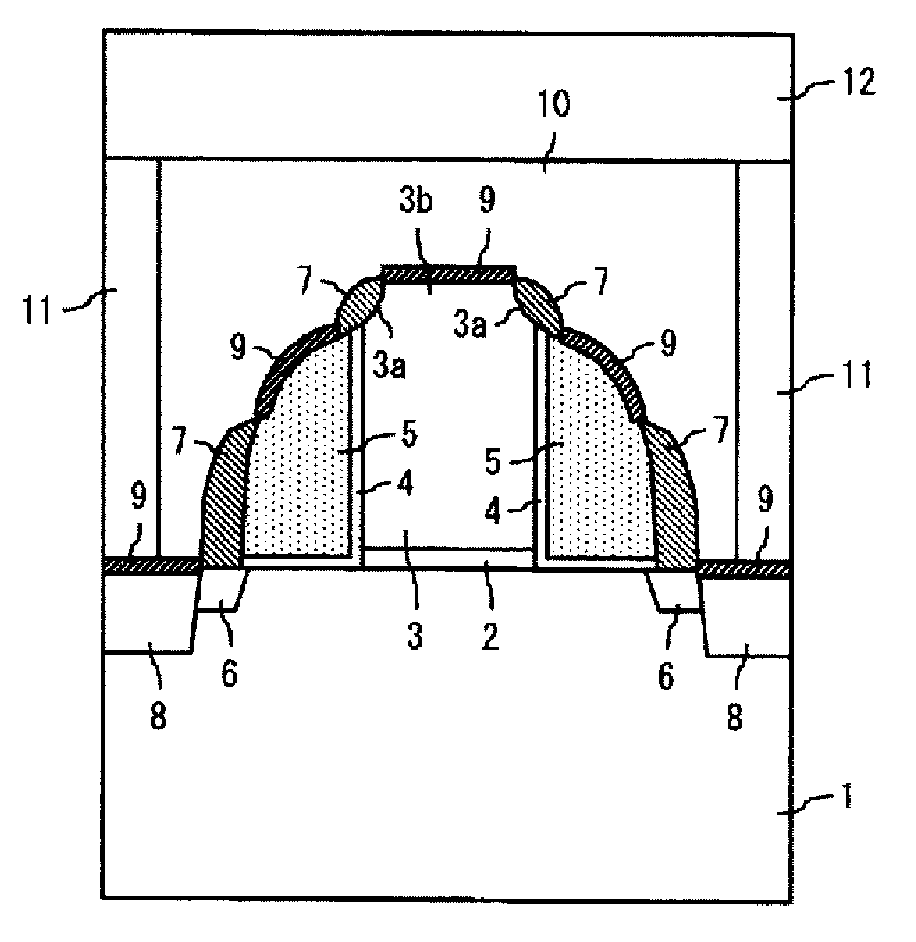
[0023]The configuration of a nonvolatile semiconductor memory device according to the first exemplary embodiment is described with reference to FIG. 1. FIG. 1 is a cross-sectional view illustrating a configuration of a nonvolatile semiconductor memory device according to the first exemplary embodiment. The nonvolatile semiconductor memory device according to this exemplary embodiment is a memory having a twin MONOS structure which a control gate 5 is formed both sides of a word gate 3.

[0024]In FIG. 1, a pair of diffusion layer 8 is provided in a main surface of a semiconductor substrate 1 as a source / drain region. The diffusion layer 8 is an n-type impurity region including such as arsenic and is formed in the surface region of the semiconductor substrate 1. A region between the pair of diffusion layer 8 is a channel region in which a channel is formed. LDD (Lightly Doped Drain) regions 6 which include an impurity at lower density than the diffusion layer 8 are provided between the ...

second exemplary embodiment

[0064]The configuration of a nonvolatile semiconductor memory device according to the second exemplary embodiment is described with reference to FIG. 4. FIG. 4 is a cross-sectional view illustrating a configuration of a nonvolatile semiconductor memory device according to the second exemplary embodiment. While, in the first exemplary embodiment, the present invention has been applied to the nonvolatile semiconductor memory device having the twin MONOS structure, in this exemplary embodiment, the example in which the present invention is applied to the nonvolatile semiconductor memory device having the structure in which the control gate 5 is only provided on one side of the word gate 3 will be described.

[0065]In FIG. 4, the word gate 3 which is the same as that in the first exemplary embodiment is formed in this exemplary embodiment. Specifically, the word gate 3 having the projecting part 3b which projects in upper direction with a certain width is formed. In this exemplary embodim...


PUM


Abstract

A nonvolatile semiconductor memory device according to an exemplary embodiment of the present invention including, a first gate electrode formed above a semiconductor substrate via a first insulating film, having a projecting part which projects in upper direction with a certain width; a second gate electrode formed beside a side surface of the first gate electrode via a second insulating film; two side walls having insulation properties formed on a side surface of the second gate electrode and a side surface of the projecting part respectively; and a silicide layer formed on an upper surface of the projecting part and a part of a surface of the second gate electrode, wherein a width of the projecting part is smaller than a width of the first gate electrode below the projecting part.

Description

INCORPORATION BY REFERENCE[0001]This application is based upon and claims the benefit of priority from Japanese patent application No. 2009-209071, filed on Sep. 10, 2009, the disclosure of which is incorporated herein in its entirety by reference.BACKGROUND[0002]1. Field of the Invention[0003]The present invention relates to a nonvolatile semiconductor memory device and a manufacturing method thereof.[0004]2. Description of Related Art[0005]Among nonvolatile semiconductor memory devices capable of programming / erasing electrically, a split gate type memory cell structure, a control gate of which is formed above a side wall of a word gate via a insulating film, as represented by the MONOS (Metal-Oxide-Nitride-Oxide-Silicon) structure is known. The word gate and the control gate are typically made of poly silicon, so each surface is alloyed (silicided) to reduce wiring resistance substantively for improving conductivity.[0006]In the split gate type MONOS memory having such configurati...

Claims


Application Information

Patent Timeline
Patent Type & Authority Applications(United States)
IPC IPC(8): H01L29/788H01L21/28
CPCH01L21/28282H01L29/42344H01L29/6656H01L29/7923H01L29/66833H01L29/7835H01L29/792H01L29/66659H01L29/40117
Inventor NAGAI, TAKAAKI
Owner RENESAS ELECTRONICS CORP
Why Eureka
Try Eureka