Nitride Semiconductor Structure and Method of Making Same

a technology of nitride and semiconductors, applied in the direction of semiconductor devices, basic electric elements, electrical apparatus, etc., can solve the problems of relatively few options to address and prevent lattice mismatch defects, crystalline defects in the material as grown, and inability to meet the requirements of bulk substrates

Active Publication Date: 2011-03-24
XEROX CORP
View PDF4 Cites 30 Cited by
  • Summary
  • Abstract
  • Description
  • Claims
  • Application Information

AI Technical Summary

Problems solved by technology

It is quite well known that when epitaxially growing a material such as a semiconductor over a substrate, a mismatch in the lattice constants of the substrate and the growth material can result in crystalline defects in the material as grown.
However, nitride materials are typically grown by metalorganic chemical vapor (MOCVD) deposition techniques onto lattice-mismatched substrates like for example sapphire, silicon carbide, and silicon for which there are relatively fewer options to address and prevent lattice mismatch defects.
However, such bulk substrates

Method used


Image

  • Nitride Semiconductor Structure and Method of Making Same
  • Nitride Semiconductor Structure and Method of Making Same
  • Nitride Semiconductor Structure and Method of Making Same

Examples


first embodiment

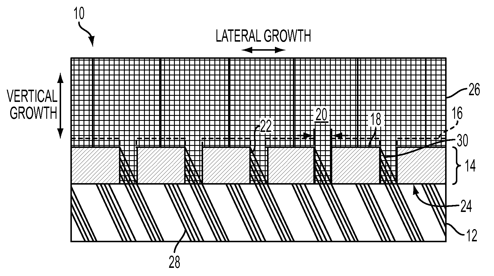
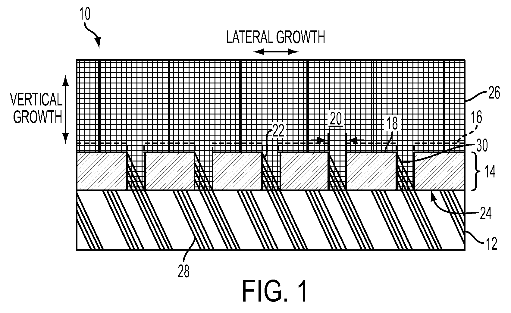
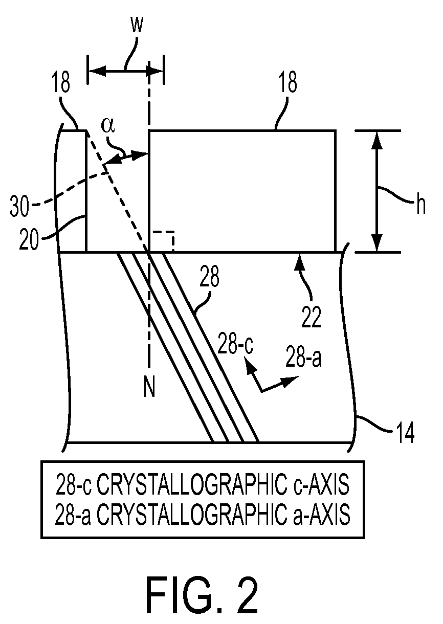
According to the present disclosure, a growth material layer is formed over a template layer. A mask is formed over the template layer, and regular “windows” are formed therein. The thickness of the masking material is selected to be greater than or equal to the product of the window width times the tangent of the angle between the surface normal and the primary plane of the template material. As the growth proceeds in the window areas, all defects tilted according to the tilt of the basal plane will be blocked by the mask.

With reference to FIG. 1, a specific example of this first embodiment is next described. A structure 10 according to this embodiment comprises a template substrate 12, which may be a 1 micron thick or thicker nitride layer (e.g., GaN, AlGaN, or InGaN or combinations thereof) of semi-polar orientation (e.g., other than (0001) or (1010) oriented surface) grown by MOCVD (or any suitable method) on sapphire or any other suitable substrate (not shown). While a gallium ...

second embodiment

In a second embodiment, the growth surface is patterned by a mask and grooves are etched into the surface with a depth greater than or equal to the product of the width of the grooves times the tangent of the angle between the surface normal and the GaN[0001] direction. This takes advantage of a large difference of growth rates along the GaN[0001] and along the opposite GaN[000-1] direction. As the former is higher and leads to defect reduction, the grooves are filled with defect-reduced material and tilted defects do not propagate to the surface.

With reference to FIG. 3, there is shown therein a structure 40 according to this second embodiment of this disclosure. Structure 40 comprises a template substrate 42, which may be a 2 micron thick or thicker nitride layer (e.g., GaN, AlGaN, or InGaN or combinations thereof) of semi-polar orientation (e.g., other than (0001) or (1010) oriented surface) grown by MOCVD (or any other suitable method) on sapphire or any other suitable substrate...

third embodiment

In a third embodiment, the growth surface is mask-patterned and grooves are etched into the surface with a depth greater than at least 0.1-0.5 μm. After etching, a masking layer is selectively deposited on all growth surfaces except for the specific facet of the grooves that points in GaN[0001] direction. This blocks any growth other than along the GaN[0001] from the highly defective seed template or substrate. Thereby, the grooves are filled with defect-reduced material and tilted defects do not propagate to the surface.

With reference to FIG. 5A, there is shown therein a structure 200 according to this third embodiment of this disclosure. Structure 200 comprises a template substrate 202, which may be a 2 micron thick or thicker nitride layer (e.g., GaN, AlGaN, or InGaN or combinations thereof) of semi-polar orientation (e.g., other than (0001) or (1010) oriented surface) grown by MOCVD (or any other suitable method) on sapphire or any other suitable substrate (not shown). A photore...


PUM


Abstract

A structure method for producing same provides suppressed lattice defects when epitaxially forming nitride layers over non-c-plane oriented layers, such as a semi-polar oriented template layer or substrate. A patterned mask with “window” openings, or trenches formed in the substrate with appropriate vertical dimensions, such as the product of the window width times the cotangent of the angle between the surface normal and the c-axis direction, provides significant blocking of all diagonally running defects during growth. In addition, inclined posts of appropriate height and spacing provide a blocking barrier to vertically running defects is created. When used in conjunction with the aforementioned aspects of mask windows or trenches, the post structure provides significant blocking of both vertically and diagonally running defects during growth.

Description

BACKGROUNDThe present disclosure is related to reducing defects which form during growth of semiconductor materials over a substrate, and more specifically to reducing certain dislocations which arise due to the lattice mismatch between a substrate and a nitride material grown thereover.It is quite well known that when epitaxially growing a material such as a semiconductor over a substrate, a mismatch in the lattice constants of the substrate and the growth material can result in crystalline defects in the material as grown. This is illustrated in FIG. 7 for a structure 100. Substrate 102 is typically oriented such that its crystal boundaries 104 are oriented roughly perpendicular to the plane of the growth surface (i.e., vertically). As a growth material 106, such as gallium nitride (GaN), forms over substrate 102, lattice defects 108 form therein which are roughly parallel to the crystal boundaries 104 of substrate 102. There are various techniques known in the art for suppressing...

Claims


Application Information

Patent Timeline
IPC IPC(8): H01L29/20H01L21/20
CPCH01L21/02389H01L21/02433H01L21/02647H01L21/02639H01L21/0254
Inventor STRITTMATTER, ANDRE
Owner XEROX CORP
Why Eureka
Try Eureka