Process to create buried heavy metal at selected depth

a heavy metal and depth technology, applied in the direction of semiconductor devices, electrical devices, transistors, etc., can solve the problems of reducing the effectiveness of lifetime killing, annealing out of silicon damage created by low doses of particle beam implants, adversely affecting other important operational parameters of the device, etc., to achieve the effect of reducing the carrier lifetime of the semiconductor devi

Inactive Publication Date: 2009-02-03
INFINEON TECH AMERICAS CORP
View PDF22 Cites 21 Cited by
  • Summary
  • Abstract
  • Description
  • Claims
  • Application Information

AI Technical Summary

Benefits of technology

[0018]It is an objective to provide reduced carrier lifetime in semiconductor devices...

Problems solved by technology

An increase of the recombination centers may adversely affect other important operational parameters of the device, such as the forward voltage drop Vce.
Damage created by electron irradiation can be uniformly distributed throughout the silicon, or can be limited to particular sites.
A disadvantage of electron irradiation is that the damage to the lattice anneals out at relatively low temperatures, thus reducing the effectiveness of the lifetime killing.
However, like E-beam irradiation, damage created by low doses of particl...

Method used


Image

  • Process to create buried heavy metal at selected depth
  • Process to create buried heavy metal at selected depth
  • Process to create buried heavy metal at selected depth

Examples


example 1

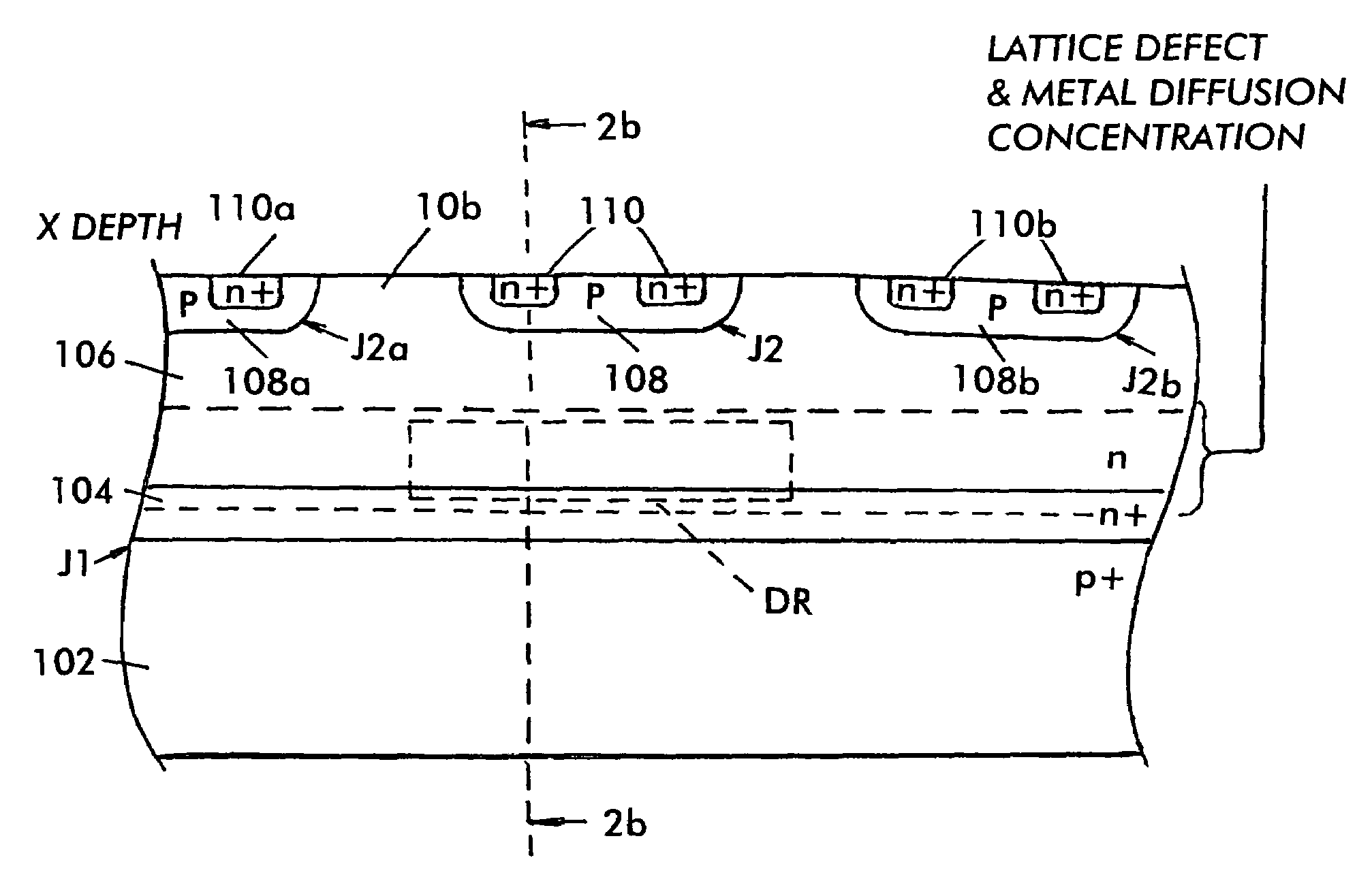
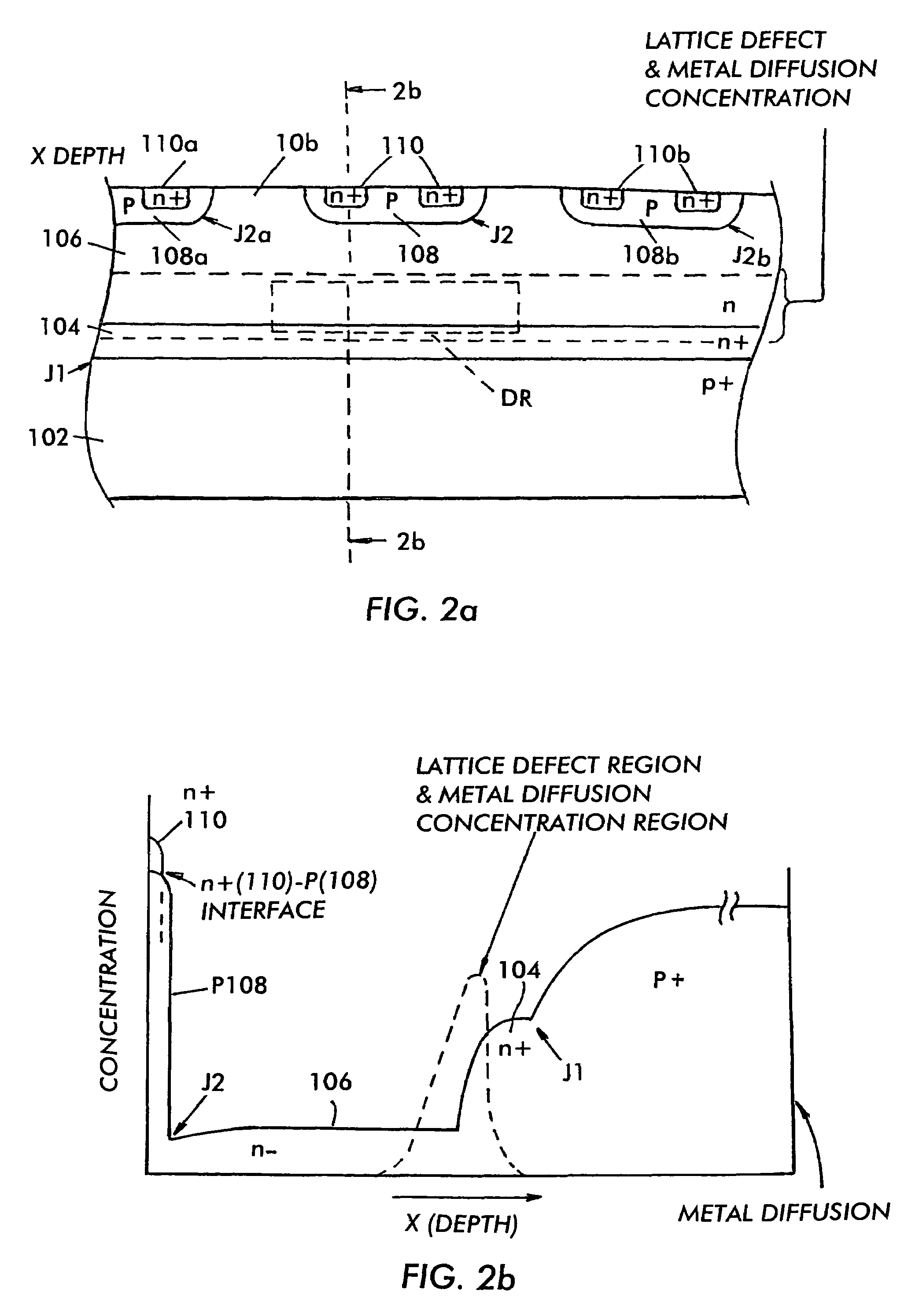
[0044]An IGBT rated for 1200V having structure as depicted in FIG. 2a and having the relative concentrations shown in FIG. 2b is constructed with the following widths:[0045]p+ substrate (102) approx. 375 microns[0046]n+ layer (104) approx. 12 microns[0047]n layer (106) approx. 100 microns[0048]p diffusion region (108) approx. 4-5 microns[0049]n+ diffusion region (110) approx. 0.3 microns

[0050]The structure is subjected to a particle beam implant of helium or hydrogen atoms through the back surface of the wafer using known techniques, dosages and energy to attain an implant profile of the concentration and position shown in FIG. 2b. The beam is applied homogeneously across the surface. The implant creates a lattice defect region across the device at the interface of n layer 106 and n+ layer 104 (i.e., peak concentration of the lattice defect region at a nominal depth of 100 microns).

[0051]The device is then subjected to metal diffusion, for example, gold, palladium or platinum, throu...

example 2

[0060]A fast recovery diode rated for 600V having structure as depicted in FIG. 3a and having the relative concentrations shown in FIG. 3b is constructed with the following widths:[0061]n+ region (202) approx. 250 microns[0062]n− region (204) approx. 60 microns[0063]p+ region (206) approx. 6 microns

[0064]Before fabrication of the anode electrode 212 and cathode electrode 210 shown in FIG. 3a, the device is subjected to a particle beam implant of helium atoms with a dose of from 5×10¹³ atoms / cm2 to 1×10¹⁵ atoms per cm2 using known techniques and appropriate energy to attain an implant profile of the concentration and position shown in FIG. 3b. The beam is applied homogeneously across the surface. This creates a lattice defect region across the device at a nominal depth Y (for the peak concentration of helium atoms) of 25 microns and a lateral width of about 15 microns.

[0065]The device is then subjected to metal diffusion. Platinum is diffused into lower n+ region at a temperature of ...

example 3

[0067]A fast recovery diode rated for 600V having structure as depicted in FIG. 3a and having the relative concentrations shown in FIG. 3b is constructed with the following widths:[0068]n+ region (202) approx. 250 microns[0069]n− region (204) approx. 60 microns[0070]p+ region (206) approx. 6 microns

[0071]Before fabrication of the anode electrode 212 and cathode electrode 210 shown in FIG. 3a, the device is subjected to a particle beam implant of helium atoms with a dosage of approximately 1×10¹² to 1×10¹⁵ atoms / cm2 using known tecniques and appropriate energy to attain an implant profile having the desired concentration and position. The beam is applied homogeneously across the surface. This creates a lattice defect region across the device at a nominal depth Y (for the peak concentration of helium atoms).

[0072]The device is then subjected to metal diffusion. Platinum is diffused into lower n+ region at a temperature of 600 to 1000° C. for 10 to 30 minutes. Again, the exact temperat...


PUM


Abstract

Semiconductor devices having recombination centers comprised of well-positioned heavy metals. At least one lattice defect region within the semiconductor device is first created using particle beam implantation. Use of particle beam implantation positions the lattice defect region(s) with high accuracy in the semiconductor device. A heavy metal implantation treatment of the device is applied. The lattice defects created by the particle beam implantation act as gettering sites for the heavy metal implantation. Thus, after the creation of lattice defects and heavy metal diffusion, the heavy metal atoms are concentrated in the well-positioned lattice defect region(s).

Description

RELATED APPLICATION[0001]This application is a continuation of U.S. application Ser. No. 09 / 593,472, filed Jun. 14, 2000 by Richard Francis and Chiu Ng entitled PROCESS TO CREATE BURIED HEAVY METAL AT SELECTED DEPTHBACKGROUND OF THE INVENTION[0002]1. Field of the Invention[0003]The invention relates to power semiconductor devices, such as insulated gate bipolar transistors (IGBTs), diodes and thyristors. In particular, the invention relates to improving performance of such devices through reduction of lifetime (also known as “lifetime killing”).[0004]2. Related Art[0005]An IGBT 10 as generally known in the art is shown in FIG. 1. The IGBT 10 has collector electrode 11 connected to a p+ collector region 12. Above collector region 12 is n+ type buffer layer 13 and n type base region 14. A pn junction is formed at interface A between collector region 12 and n+ buffer layer 13. Typically, p+ collector region 12 is formed in the semiconductor wafer, while n+ buffer layer and n base regio...

Claims


Application Information

Patent Timeline
IPC IPC(8): H01L29/02H01L21/22H01L21/263H01L21/265H01L21/329H01L21/331H01L29/167H01L29/32
CPCH01L21/221H01L21/263H01L21/26506H01L29/167H01L29/32H01L29/66136H01L29/66333
Inventor FRANCIS, RICHARDNG, CHIU
Owner INFINEON TECH AMERICAS CORP
Why Eureka
Try Eureka