

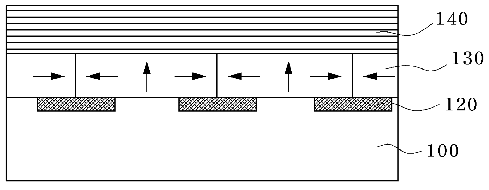
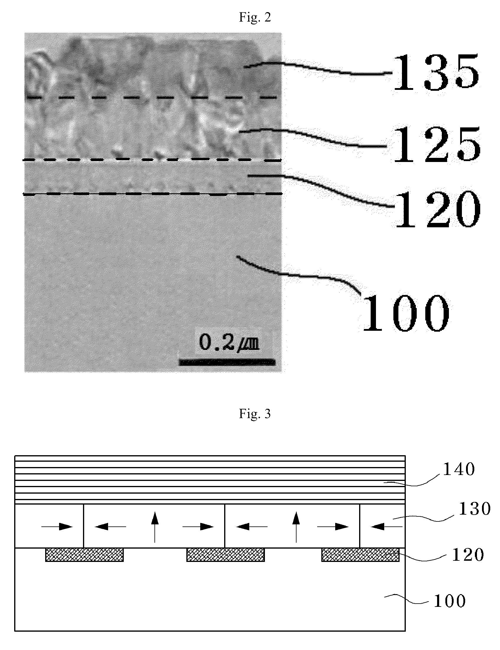
Method of forming nitride semiconductor and electronic device comprising the same
a technology of nitride and semiconductor, which is applied in the direction of semiconductor devices, semiconductor lasers, lasers, etc., can solve the problems of deteriorating quality of gallium nitride thin film, mismatch dislocation, and difficulty in fabricating gan thin film into bulk-type single crystal substrate such as ingots, and achieve the effect of facilitating the growth of metal nitride thin film 130
- Summary
- Abstract
- Description
- Claims
- Application Information
AI Technical Summary
Benefits of technology
Problems solved by technology
Method used
Image

Examples
example 1
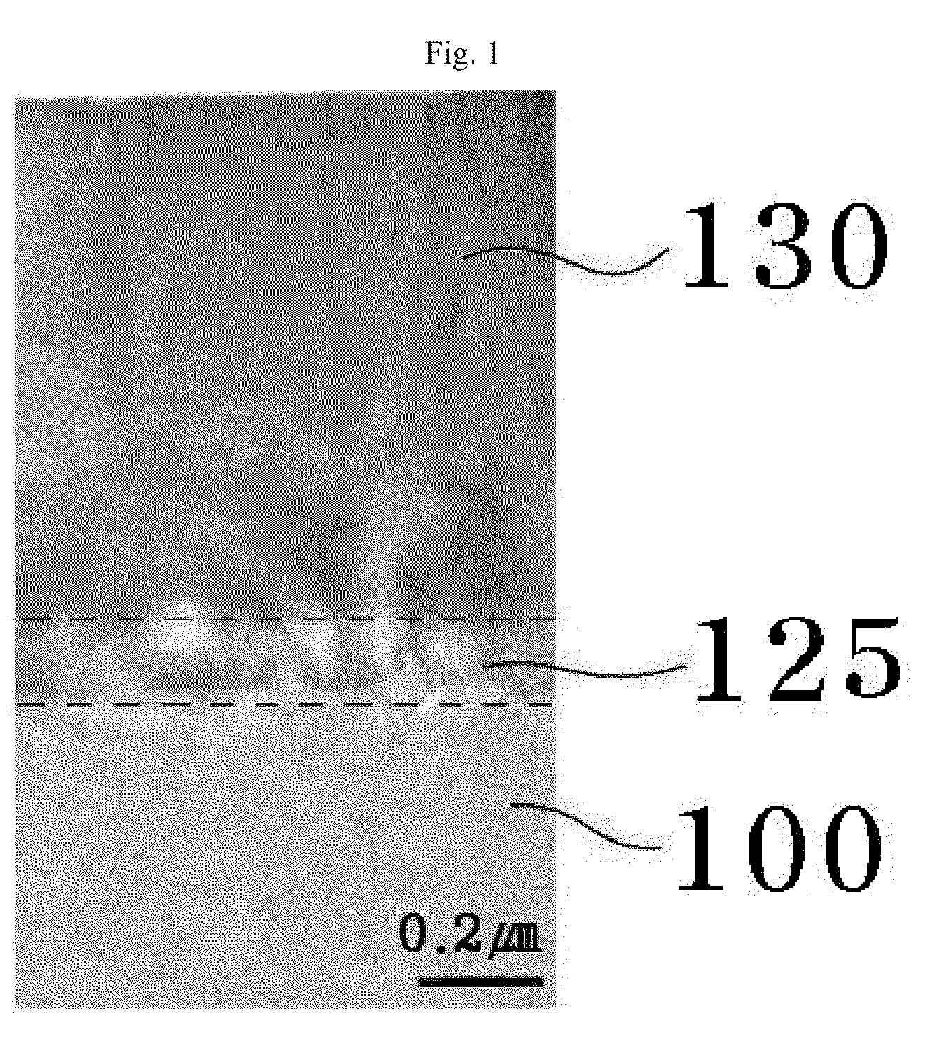
[0060]First, an ion implantation region of a line / space pattern is formed on a single crystal silicon substrate by the method according to the present invention. Here, a space pattern had a width of 11 μm and a line pattern given as an ion implantation region had a width of 5 μm.
[0061]Then, after forming an ion implantation mask of 10 μm thickness on the silicon substrate, ion implantation was performed to a thickness of 100 nm at a nitrogen ion dose of 5E17 ion / cm2 at an ion implantation energy of 37.5 keV.
[0062]Then, after removing the mask from the silicon substrate, the silicon substrate was washed using acetone, methanol, and deionized water in this order, and was then dried using nitrogen gas.
[0063]Next, an AlN layer of 100 μm thickness and a GaN thin film of 1˜1.2 μm thickness were sequentially formed on the dried silicon substrate within an MOCVD chamber.
[0064]FIGS. 6a to 6c are SEM micrographs showing an upper surface and a cross-section of a GaN thin film of Example 1 duri...
PUM
| Property | Measurement | Unit |
|---|---|---|
| energy | aaaaa | aaaaa |
| depth | aaaaa | aaaaa |
| band gap | aaaaa | aaaaa |
Abstract
Description
Claims
Application Information