Forming radio frequency integrated circuits

a technology of integrated circuits and radio frequency, which is applied in the direction of semiconductor devices, semiconductor/solid-state device details, electrical apparatus, etc., can solve the problems of significant limitation on further reducing the form factor of rfic, material and processing conditions in the existing cmos process flow are not tailored for the ideal performance of on-chip inductors, and none of the existing solutions are without pitfalls

Active Publication Date: 2011-03-24
QUALCOMM INC
View PDF11 Cites 285 Cited by
  • Summary
  • Abstract
  • Description
  • Claims
  • Application Information

AI Technical Summary

Benefits of technology

[0009]In a further preferred embodiment, a method of forming an RFIC in an Passive-On-Glass (POG) package comprises the steps of forming a plurality of electronic devices and one or more TSVs in a semiconductor wafer, forming an electrical shield structure in a re-distribution (RDL) layer on a first surface of the semiconductor wafer, and forming one or more passive devices on a top surface of a dielectric substrate. The method also comprises bonding the dielectric substrate to the semiconductor wafer at the first surface of the semiconductor wafer and the top surface of a dielectric substrate, forming a stacking wafer structure. The method further comprises bonding the stacking wafer structure to a POG package substrate at a second surface of the semiconductor wafer.
[0010]In an additional preferred embodiment, an RFIC in a POG package configuration comprises one or more microelectronic devices and one or more through-silicon-vias (TSVs) in a semiconductor substrate. The RFIC also comprises one or more passive devices on a dielectric substrate, wherein the dielectric substrate is bonded to the semiconductor substrate in a stacking manner, and wherein the one or more passive devices is electrically coupled to the one or more microelectronic device through the one or more TSVs. The RFIC further comprises means for shielding the one or more microelectronic devices from the one or more passive devices.

Problems solved by technology

Although widely used, this existing approach of fabricating RF front module poses a few drawbacks.
First, materials and processing conditions in an existing CMOS process flow are not tailored for the ideal performance of on-chip inductors.
Second, in current practice, the silicon areas under the on-chip inductors are typically left blank in an effort to avoid the undesirable eddy currents induced in the silicon substrate due to the varying magnetic flux from the on-chip inductors.
This drawback poses a significant limitation on further reducing the form factor of an RFIC.
Although temporary solutions have been proposed, none of the existing solutions are without pitfalls.
These horizontal feed-throughs, however, generally increase the footprint size of an RFIC.
Among other drawbacks of the existing approach, horizontal feed-throughs create crossing signal lines that may affect circuit performance, lengthy horizontal signal line routings may increase signal latency, and long metal traces may lead to undesirable inductance.

Method used


Image

  • Forming radio frequency integrated circuits
  • Forming radio frequency integrated circuits
  • Forming radio frequency integrated circuits

Examples


Embodiment Construction

[0019]The making and using of the presently preferred embodiments are discussed in detail below. It should be appreciated, however, that the present invention provides many applicable inventive concepts that can be embodied in a wide variety of specific contexts. The specific embodiments discussed are merely illustrative of specific ways to make and use the invention, and do not limit the scope of the invention.

[0020]The present invention will be described with respect to preferred embodiments in a specific context, namely method of making RF integrated circuits (RFICs) in a Passive-On-Glass (POG) configuration. However, features, methods, structures or characteristics described according to the preferred embodiments may also be combined in suitable manners to form one or more other embodiments. Also, for clarification, the figures are drawn only to illustrate the relevant aspects of the inventive features or characteristics, and are not drawn to scale.

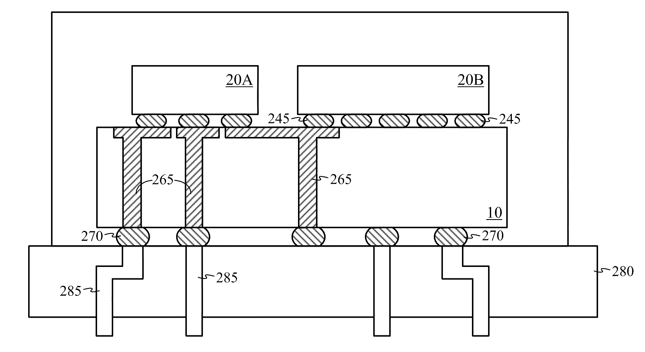
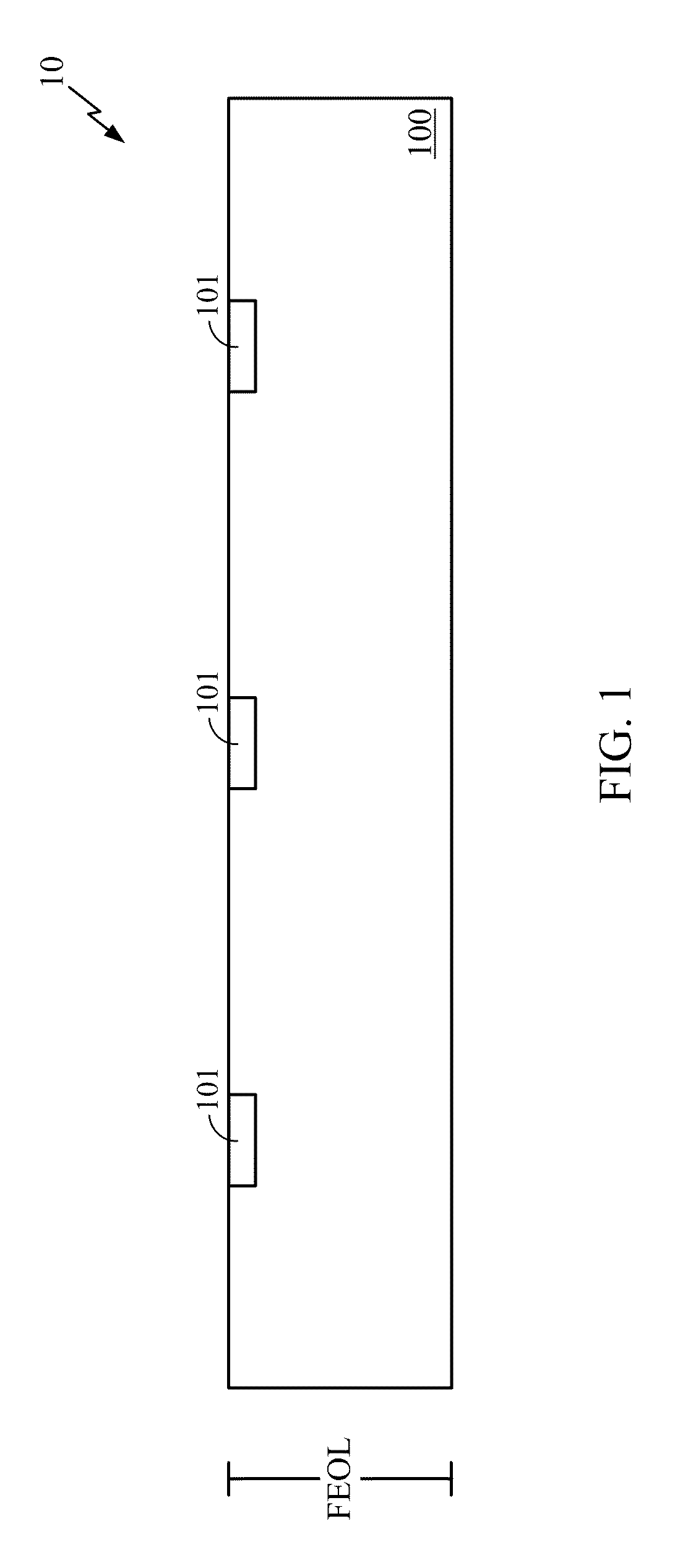
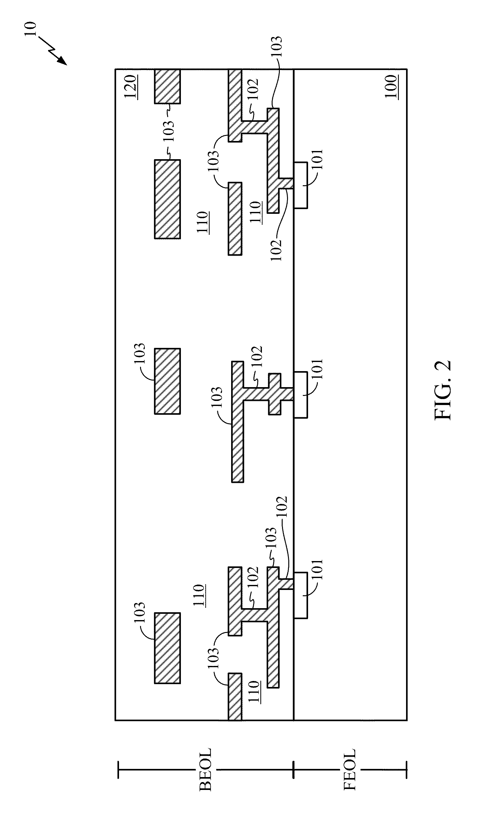
[0021]With reference now to FI...


PUM


Abstract

Method of forming a radio frequency integrated circuit (RFIC) is provided. The RFIC comprises one or more electronic devices formed in a semiconductor substrate and one or more passive devices on a dielectric substrate, arranged in a stacking manner. Electrical shield structure is formed in between to shield electronic devices in the semiconductor substrate from the passive devices in the dielectric substrate. Vertical through-silicon-vias (TSVs) are formed to provide electrical connections between the passive devices in the dielectric substrate and the electronic devices in the semiconductor substrate.

Description

TECHNICAL FIELD[0001]The present invention relates in general to radio frequency (RF) microelectronic devices and more particularly to forming RF integrated circuitry (RFIC) in a Passive-On-Glass (POG) configuration.BACKGROUND[0002]Wireless communication technology and its applications have made tremendous influences in various aspects of modern society. In the past decades, numerous technical breakthroughs have been realized in wireless communication techniques. These advances are represented by the wide adoption of highly efficient access techniques, such as code division multiple access (CDMA), the integration of digital coding / decoding and digital signal processing techniques into a wireless communication device, and the rapid progress in semiconductor manufacturing techniques that enables integrating a large amount of microelectronic circuits on a semiconductor integrated circuit (IC) die. These progresses have led to wireless communication products of today's, such as a mobile...

Claims


Application Information

Patent Timeline
Patent Type & Authority Applications(United States)
IPC IPC(8): H01L25/16H01L21/02H01L21/50
CPCH01L23/552H01L23/645H01L2924/1305H01L2924/10253H01L2924/13091H01L2224/16H01L2924/01079H01L2924/09701H01L2924/15311H01L2924/19011H01L2924/19104H01L2924/3025H01L2924/00H01L2224/16265H01L2224/0401H01L2224/05567H01L2224/0557H01L2224/06181H01L2224/13025H01L2224/16235H01L2224/17181
Inventor KIM, JONGHAEHENDERSON, BRIAN M.NOWAK, MATTHEW M.XU, JIAYU
Owner QUALCOMM INC
Why Eureka
Try Eureka