Capacitance touch panel module and fabrication method thereof

a touch panel module and capacitance technology, applied in the manufacture of electric discharge tubes/lamps, pulse techniques, instruments, etc., can solve the problems of reducing quality, reducing light transmittance, and overly thick units with less than the optimum light transmittance,

Active Publication Date: 2011-03-24
INNOCOM TECH SHENZHEN +1
View PDF4 Cites 61 Cited by
  • Summary
  • Abstract
  • Description
  • Claims
  • Application Information

AI Technical Summary

Problems solved by technology

The conventional touch panel module having five layers, in combination with a possibly-added cover lens, results in an overly thick un...

Method used


Image

  • Capacitance touch panel module and fabrication method thereof
  • Capacitance touch panel module and fabrication method thereof
  • Capacitance touch panel module and fabrication method thereof

Examples


first embodiment

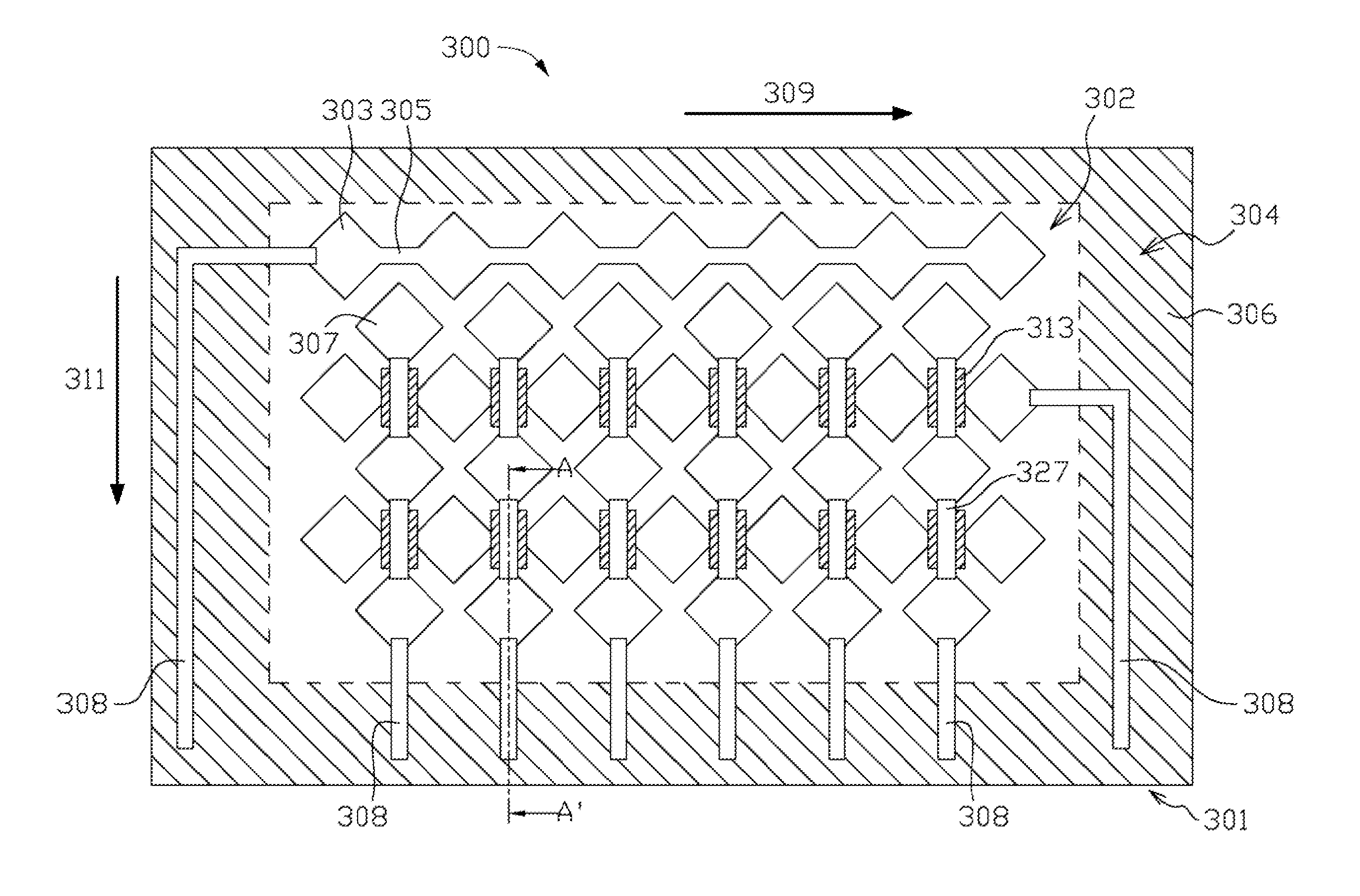
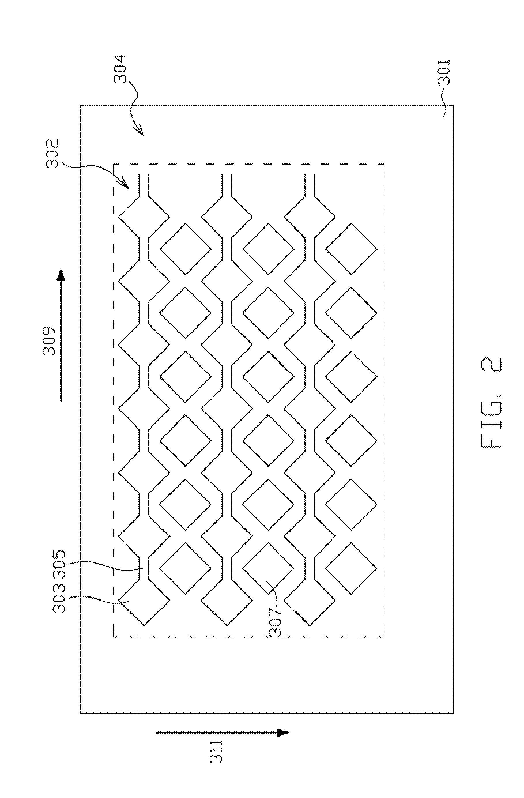
[0010]Referring to FIGS. 1 and 2, a method of fabricating a capacitance touch panel module is described as follows. A substrate 301 with a touching area 302 and a peripheral area 304 arranged around the touching area 302 is provided. The substrate 301 may be made of glass, quartz, plastic, resin, acrylic fabric, or other transparent material.

[0011]A transparent conductive layer (not shown) is formed on the substrate 301 of indium tin oxide (ITO), indium zinc oxide (IZO), aluminum zinc oxide (AZO), gallium zinc oxide (GZO), magnesium indium oxide (MIO), or other transparent conductive materials. The transparent conductive layer is etched to form a plurality of first conductive patterns 303, a plurality of second conductive patterns 307, and a plurality of connecting portions 305 in the touching area 302. The first conductive patterns 303 are arranged in a plurality of rows along a first orientation 309. The second conductive patterns 307 are arranged between the neighboring rows of t...

second embodiment

[0018]Referring to FIGS. 6 and 7, a method of fabricating a capacitance touch panel module is described as follows. A substrate 401 with a touching area 402 and a peripheral area 404 arranged around the touching area 402 is provided. A plurality of bridging members 427 is formed in the touching area 402.

[0019]Referring to FIG. 8, a plurality of insulated protrusions 413 is formed in the touching area 402. Each insulated protrusion 413 covers at least part of one bridging member 427. An insulated frame 406 is formed in the peripheral area 404. The insulated protrusions 413 and the insulated frame 406 are formed as disclosed in the first embodiment.

[0020]Referring to FIG. 9, a transparent conductive layer (not shown) is formed on the substrate 401, for supporting a plurality of first conductive patterns 403, a plurality of second conductive patterns 407, and a plurality of connecting portions 405 in the touching area 402. The arrangement of the first conductive patterns 403, the secon...


PUM

PropertyMeasurementUnit
Electrical conductoraaaaaaaaaa
Areaaaaaaaaaaa
Lightaaaaaaaaaa

Abstract

A method of fabricating a capacitance touch panel module includes forming a plurality of first conductive patterns on a substrate comprising a touching area and a peripheral area along a first orientation, a plurality of second conductive patterns along a second orientation, and a plurality of connecting portions in the touching area; forming a plurality of insulated protrusions, in which each insulated protrusion covering one connecting portion, and forming an insulated frame on the peripheral area; and forming a bridging member on each insulated protrusion.

Description

BACKGROUND[0001]1. Technical Field[0002]The present disclosure generally relates to capacitance touch panel modules, and particularly, to a capacitance touch panel module and a fabrication method thereof.[0003]2. Description of Related Art[0004]Capacitance touch panels are often used in portable electronic devices due to their dustproof, multi-touch capabilities, and thermostable properties.[0005]A commonly used capacitance touch panel module includes a touch panel and a cover lens bonded thereto by using optical adhesive. The touch panel includes a base plate, two transparent conductive layers, and two insulating layers. The conventional touch panel module having five layers, in combination with a possibly-added cover lens, results in an overly thick unit having lesser than optimum light transmittance, and reduced quality. In addition, the optical adhesive is expensive and cannot be recycled.[0006]Therefore, there is room for improvement within the art.BRIEF DESCRIPTION OF THE DRAW...

Claims


Application Information

Patent Timeline
IPC IPC(8): G06F3/045H01J9/00
CPCG06F3/044Y10T29/49162G06F2203/04103H05K1/0274H05K1/0306H05K3/10H05K3/125H05K2201/0108H05K2201/017H03K17/9622H03K2017/9613H03K2217/96075H03K2217/960765G06F2203/04111H03K2217/960755Y10T29/49105Y10T29/49155G06F2203/041H05K1/0296G06F2203/04112G06F3/0443G06F3/0446
Inventor MENG, KAILEE, LIEN-HSIN
Owner INNOCOM TECH SHENZHEN
Why Eureka
Try Eureka