Method for polishing through-silicon via (TSV) wafers and a polishing composition used in the method

a technology of silicon via and polishing composition, which is applied in the direction of lapping machines, manufacturing tools, aqueous dispersions, etc., can solve the problems of not being able to directly polish affecting conductive materials, and reducing the polishing rate of silicon via and conductive materials, so as to achieve reliable polishing

Active Publication Date: 2011-03-24
ENTEGRIS INC
View PDF3 Cites 8 Cited by
  • Summary
  • Abstract
  • Description
  • Claims
  • Application Information

AI Technical Summary

Benefits of technology

[0012]The inventors of the present application attempted to use sodium chlorite or potassium bromate as the oxidizing agent and sodium chlorite and / or potassium bromate in combination with an organic alkaline compound as the components of a polishing composition. Surprisingly, the formulated polishing composition shows excellent polishing effects on both silicon and conductive materials. It is confirmed through experiments that the removal rates for both substances simultaneously can even exceed 9,500 Å / min under machine operating conditions in which the polishing pressure is less than 3 psi, and the rotation rates of the polishing pad and the polishing head are less than 100 rpm.
[0013]A first objective of the present invention is to provide a polishing method which can simultaneously and rapidly remove conductive materials and silicon on a TSV wafer to be polished. The polishing method comprises subjecting the surface of a TSV wafer to a polishing treatment with a polishing composition to simultaneously remove Si and conductive material on the TSV wafer at their respective removal rates, wherein the polishing composition comprises an organic alkaline compound, an oxidizing agent selected from a chlorite salt and / or bromated salt, silicon oxide abrasive particles and a solvent.
[0015]By the method of the present invention and the polishing composition used therein, the silicon and conductive materials on a TSV wafer are simultaneously removed in a more acceptable rate without using hydrogen peroxide. A novel and reliable polishing method and polishing composition for the CMP process of the TSV wafer are also provided.

Problems solved by technology

Thus, for manufacturers who need to polish a substantial amount of TSV wafers, if both the silicon wafer layer 12 and the conductive materials 13 can be simultaneously and rapidly removed to a suitable status, it may save a very considerable working-hour cost in the manufacturing process.
However, the commercially available polishing compositions are mainly designed for common silicon wafers composed of only one single material, either silicon or a conductive material, and are not suitable for directly polishing a TSV wafer.
When simultaneously polishing silicon and conductive materials, the removal rates for the two substances are very different from each other, and therefore, it is difficult to increase the polishing rates for silicon and the conductive material simultaneously by increasing the amount of one specific ingredient in the polishing composition.
Similarly, the oxidizing agent hydrogen peroxide widely used in the polishing composition may be useful for polishing the conductive materials; however, it may easily oxidize silicon to hard silica.
Accordingly, hydrogen peroxide is not considered to be suitable as an ingredient of the polishing composition for simultaneously polishing silicon and a conductive material.

Method used


Image

  • Method for polishing through-silicon via (TSV) wafers and a polishing composition used in the method
  • Method for polishing through-silicon via (TSV) wafers and a polishing composition used in the method

Examples


Embodiment Construction

[0019]The method for polishing a TSV wafer according to the present invention is to subject one surface of the TSV wafer to a polishing treatment with the aforesaid polishing composition of the present invention. During the polishing treatment, the polishing composition flows towards the polishing pad and the TSV wafer at a certain flow rate at the same time that the TSV wafer comes into contact with the polishing pad with a polishing pressure. The TSV wafer and the polishing pad respectively have their rotation rates to polish the TSV wafer.

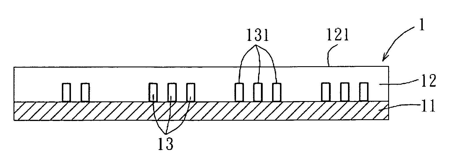
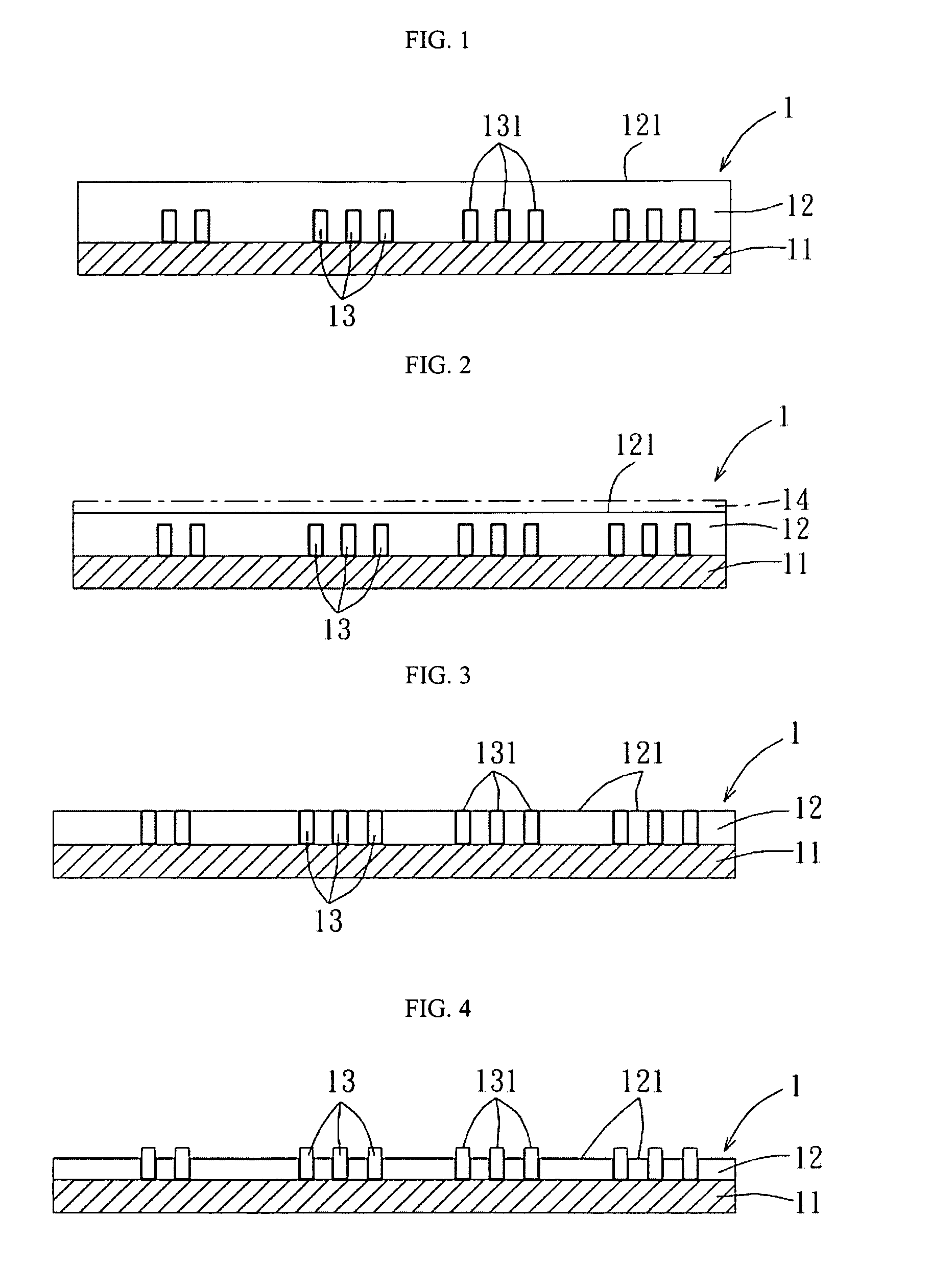
[0020]It should be first clarified that the “surface of the TSV wafer” means the surface of the TSV wafer that is farthest away from integrated circuit layer 11 and may be surface 121 of the silicon wafer layer (as shown in FIG. 1) or cover end surfaces 131 of conductive materials 13 (as shown in FIG. 3).

[0021]With such an operation, the removal rates of the conductive material and silicon on a TSV wafer can both exceed 6,000 Å / min, even 8,000 Å...


PUM

PropertyMeasurementUnit
pressureaaaaaaaaaa
compositionaaaaaaaaaa
conductiveaaaaaaaaaa

Abstract

A method for polishing Through-Silicon Via (TSV) wafers is provided. The method comprises a step of subjecting the surface of a TSV wafer to a polishing treatment with a polishing composition containing an organic alkaline compound, an oxidizing agent selected from sodium chlorite and / or potassium bromate, silicon oxide abrasive particles, and a solvent to simultaneously remove Si and conductive materials at their respective removal rates. By using the method of this invention, Si and conductive materials can be simultaneously polished at higher removal rates to significantly save the necessary working-hour costs for polishing TSV wafers. A polishing composition used in the above method is also provided.

Description

FIELD OF THE INVENTION[0001]The present invention relates to a polishing method, especially, a method for polishing a through-silicon via (TSV) wafer. The present invention also relates to a polishing composition used for conducting the method.BACKGROUND OF THE INVENTION[0002]FIG. 1 shows the original structure of a TSV wafer 1, which comprises an integrated circuit layer 11, a silicon wafer layer 12 arranged on integrated circuit layer 11, and conductive materials 13. Conductive materials 13 are buried in silicon wafer layer 12, are approximately perpendicular to surface 121 of silicon wafer layer 12, and connect to integrated circuit layer 11. Generally, end surfaces 131 of conductive materials 13 in an unpolished TSV wafer are about a couple hundred micrometers from surface 121 of silicon wafer layer 12.[0003]Surface 121 is subsequently polished by grinding, so that silicon wafer layer 12 is rapidly thinned, and thereby the distance between end surfaces 131 of conductive material...

Claims


Application Information

Patent Timeline
Patent Type & Authority Applications(United States)
IPC IPC(8): H01L21/302C09K13/00B24B37/00H01L21/304
CPCH01L21/30625C09G1/02C09G1/04H01L21/304H01L21/3212H01L21/76898
Inventor LEE, KANG-HUALIU, WEN-CHENG
Owner ENTEGRIS INC
Why Eureka
Try Eureka